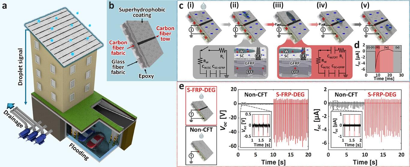
БЛОГ

Archive for the ‘engineering’ category: Page 10

Oct 11, 2023

Research shows how topology can help create magnetism at higher temperatures

Posted by in categories: engineering, quantum physics

Researchers who have been working for years to understand electron arrangement and magnetism in certain semimetals have been frustrated by the fact that the materials only display magnetic properties if they are cooled to just a few degrees above absolute zero.

A new MIT study led by Mingda Li, associate professor of nuclear science and engineering, and co-authored by Nathan Drucker, a graduate research assistant in MIT’s Quantum Measurement Group and Ph.D. student in applied physics at Harvard University, along with Thanh Nguyen and Phum Siriviboon, MIT graduate students working in the Quantum Measurement Group, is challenging that conventional wisdom.

The open-access research, published in Nature Communications, for the first time shows evidence that topology can stabilize , even well above the magnetic transition temperature—the point at which normally breaks down.

Oct 11, 2023

Toward metropolitan free-space quantum networks

Posted by in categories: engineering, internet, quantum physics

Quantum communications have rapidly progressed toward practical, large-scale networks based on quantum key distributions that spearhead the process. Quantum key distribution systems typically include a sender “Alice,” a receiver “Bob,” who generate a shared secret from quantum measurements for secure communication. Although fiber-based systems are well-suited for metropolitan scale, a suitable fiber infrastructure might not always be in place.

In a new report in npj Quantum Information, Andrej Kržič and a team of scientists developed an entanglement-based, free-space quantum . The platform offered a practical and efficient alternative for metropolitan applications. The team introduced a free-space quantum key distribution system to demonstrate its use in realistic applications in anticipation of the work to establish free-space networks as a viable solution for metropolitan applications in the future global quantum internet.

Quantum communication typically aims to distribute quantum information between two or more parties. A series of revolutionary applications of quantum networks have provided a roadmap towards engineering a full-blown quantum internet. The proposed invention provides a heterogeneous network of special purpose sub-networks with diverse links and interconnects. The concept of quantum key distribution networks have driven this development to pave the way for other distributed processing methods to benchmark the technological maturity of quantum networks in general.

Oct 9, 2023

Giant wind turbine erected in just 30 hours signifies major engineering feat: ‘This can save about 500,000 tons of standard coal’

Posted by in categories: energy, engineering, sustainability

Wind turbines are a feat of engineering. The massive structures are visually impressive and generate vast amounts of clean energy via a natural and pollution-free source.

Because of that, you’d think they take a long time to install — especially when placed far out at sea.

However, at an offshore wind farm in Zhangpu, China, the state-owned China Three Gorges power company managed to get one up and running in just over a day, Electrek reports.

Oct 9, 2023

Promptbreeder: Self-Referential Self-Improvement Via Prompt Evolution (Paper Explained)

Posted by in categories: engineering, evolution, information science

#evolution.

Promptbreeder is a self-improving self-referential system for automated prompt engineering. Give it a task description and a dataset, and it will automatically come up with appropriate prompts for the task. This is achieved by an evolutionary algorithm where not only the prompts, but also the mutation-prompts are improved over time in a population-based, diversity-focused approach.

Continue reading “Promptbreeder: Self-Referential Self-Improvement Via Prompt Evolution (Paper Explained)” »

Oct 8, 2023

High-strength and ultra-tough whole spider silk fibers spun from transgenic silkworms

Posted by in categories: cyborgs, engineering, sustainability, transhumanism

Lightweight materials with super strength and toughness are highly sought after. Spider silk, a sustainable material, meets these requirements but faces challenges in commercialization due to scientific understanding of its spinning mechanism, technical complexities in the process, and engineering hurdles in low-cost mass production. Here, drawing inspiration from nylon and Kevlar, we propose a theory on the nature of toughness and strength, unveiling the basic structure of silk fibers. Using these theories, we successfully produce the first “localized” full-length spider silk fiber via transgenic silkworms, showcasing high tensile strength (1,299 MPa) and exceptional toughness (319 MJ/m3). This breakthrough overcomes scientific, technical, and engineering obstacles, paving the way for spider silk’s commercialization as a sustainable substitute for synthetic fibers. Moreover, our theories provide essential guidance for developing super materials.


Developing sustainable materials with high strength and ultra-toughness is vital for ecological civilization. Using transgenic silkworms, we have successfully produced the first full-length spider silk, overcoming the scientific challenge of understanding the essence of toughness and strength. The resulting bionic spider silk exhibits high strength (1,299 MPa) and ultra-toughness (319 MJ/m3), offering a potentially sustainable substitute for synthetic commercial fibers. This breakthrough provides valuable insights for the development of super materials, including those for a space elevator, driving the advancement of civilization.

Oct 8, 2023

Reflecting sunlight to cool the planet will cause other global changes

Posted by in category: engineering

MIT researchers find that extratropical storm tracks would change significantly with solar geoengineering efforts.

Oct 7, 2023

Free-space nanoprinting beyond optical limits to create 4D functional structures

Posted by in categories: biotech/medical, engineering, nanotechnology

Two-photon polymerization is a potential method for nanofabrication to integrate nanomaterials based on femtosecond laser-based methods. Challenges in the field of 3D nanoprinting include slow layer-by-layer printing and limited material options as a result of laser-matter interactions.

In a new report now on Science Advances, Chenqi Yi and a team of scientists in Technology Sciences, Medicine, and Industrial Engineering at the Wuhan University China and the Purdue University U.S., showed a new 3D nanoprinting approach known as free-space nanoprinting by using an optical brush.

This concept allowed them to develop precise and spatial writing paths beyond optical limits to form 4D functional structures. The method facilitated the rapid aggregation and solidification of radicals to facilitate polymerization with increased sensitivity to , to provide high accuracy, free-space painting much like Chinese brush painting on paper.

Oct 6, 2023

Controlling Hydrogen Isotopes with Graphene

Posted by in categories: engineering, nuclear energy, particle physics

face_with_colon_three Year 2017


A paper recently published in the journal Nuclear Engineering and Technology demonstrated the feasibility of using graphene to control hydrogen isotopes, specifically tritium.

Study: Adsorption of Hydrogen Isotopes on Graphene. Image Credit: Rost9/Shutterstock.com

Continue reading “Controlling Hydrogen Isotopes with Graphene” »

Oct 5, 2023

Inspired by butterfly wings, researchers develop a soft, color-changing system for optical devices

Posted by in categories: biotech/medical, engineering, mobile phones, wearables

Researchers at the University of Hong Kong (HKU) have designed an innovative pixelated, soft, color-changing system called a Morphable Concavity Array (MoCA).

Pixelated, soft, color-changing systems are malleable structures that can change color by manipulating light. They have applications in a wide range of industries, from medical bandages that change color if there is an infection, to foldable screens on smartphones and tablets, as well as wearable technology where sensors are integrated into the clothing fabric.

The research was co-directed by Professor Anderson Ho Cheung Shum from the Department of Mechanical Engineering at HKU, and Professor Mingzhu Li from the Institute of Chemistry, Chinese Academy of Sciences, and led by Dr. Yi Pan from the Department of Mechanical Engineering at HKU.

Oct 5, 2023

Quantum repeaters use defects in diamond to interconnect quantum systems

Posted by in categories: computing, engineering, particle physics, quantum physics

Ben Dixon, a researcher in the Optical and Quantum Communications Technology Group, explains how the process works: “First, you need to generate pairs of specific entangled qubits (called Bell states) and transmit them in different directions across the network link to two separate quantum repeaters, which capture and store these qubits. One of the quantum repeaters then does a two-qubit measurement between the transmitted and stored qubit and an arbitrary qubit that we want to send across the link in order to interconnect the remote quantum systems. The measurement results are communicated to the quantum repeater at the other end of the link; the repeater uses these results to turn the stored Bell state qubit into the arbitrary qubit. Lastly, the repeater can send the arbitrary qubit into the quantum system, thereby linking the two remote quantum systems.”

To retain the entangled states, the quantum repeater needs a way to store them — in essence, a memory. In 2020, collaborators at Harvard University demonstrated holding a qubit in a single silicon atom (trapped between two empty spaces left behind by removing two carbon atoms) in diamond. This silicon “vacancy” center in diamond is an attractive quantum memory option. Like other individual electrons, the outermost (valence) electron on the silicon atom can point either up or down, similar to a bar magnet with north and south poles. The direction that the electron points is known as its spin, and the two possible spin states, spin up or spin down, are akin to the ones and zeros used by computers to represent, process, and store information. Moreover, silicon’s valence electron can be manipulated with visible light to transfer and store a photonic qubit in the electron spin state. The Harvard researchers did exactly this; they patterned an optical waveguide (a structure that guides light in a desired direction) surrounded by a nanophotonic optical cavity to have a photon strongly interact with the silicon atom and impart its quantum state onto that atom. Collaborators at MIT then showed this basic functionality could work with multiple waveguides; they patterned eight waveguides and successfully generated silicon vacancies inside them all.

Lincoln Laboratory has since been applying quantum engineering to create a quantum memory module equipped with additional capabilities to operate as a quantum repeater. This engineering effort includes on-site custom diamond growth (with the Quantum Information and Integrated Nanosystems Group); the development of a scalable silicon-nanophotonics interposer (a chip that merges photonic and electronic functionalities) to control the silicon-vacancy qubit; and integration and packaging of the components into a system that can be cooled to the cryogenic temperatures needed for long-term memory storage. The current system has two memory modules, each capable of holding eight optical qubits.

Page 10 of 228First7891011121314Last