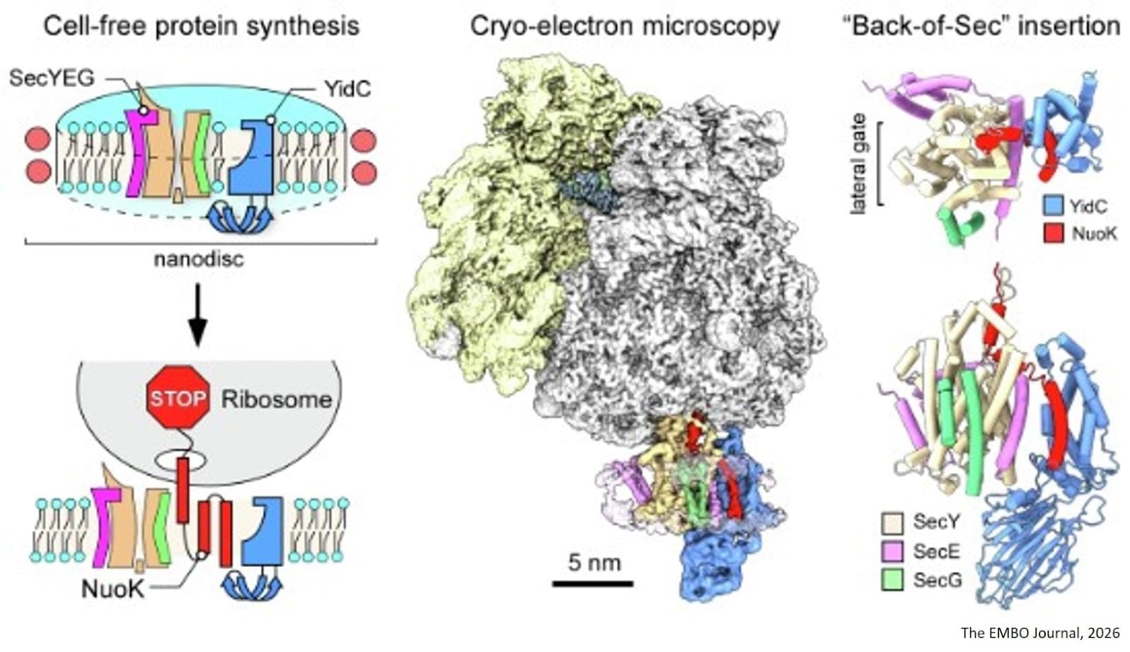
The cell membrane contains a large number of proteins, which perform a wide variety of functions. Some serve as transport channels, specifically guiding substances into the cell or carrying cellular products out of it. Others are receptors, which detect control signals and then trigger processes in the cell. These proteins are folded in complex three-dimensional structures, with the specific form essential for the protein function.
One question remains unanswered in many cases for researchers: How do the proteins manufactured by the ribosomes – the “factories” of the cells – in the cell interior reach their position within the membrane in the correct form and when did the processes become established over the course of evolution?
For those who have enjoyed Westworld and other Sci-fi movies and writings of high quality that have imagined digital beings, robots, like humans, I give you “The Specification”. I have worked for weeks on this, if not years imaging it, and it kind of makes sense. I give it freely. It is what it is, I take no responsibility for birthing the document which creates a digital virtual human being! Not joking actually…
VHOS —A generic OS for capturing, modeling, and re-instantiating “virtual human beings” across successive generations of AI — the Virtual Human Operating System.
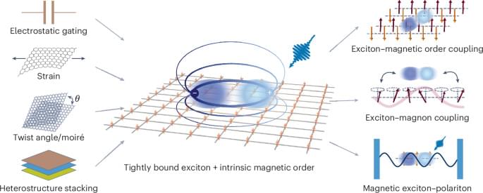
Two-dimensional magnetic semiconductors provide a unique platform where long-range magnetic order coexists with strongly bound excitons. Because excitonic states and magnetic moments originate from the same electronic orbitals and couple via intrinsic exchange interactions, optical excitations in these systems exhibit pronounced sensitivity to magnetic order. Recent experiments show unusually strong magneto-optical responses and direct exciton–magnon coupling, establishing new routes for controlling light–matter interactions with spin degrees of freedom. This Review surveys key developments, focusing on representative material systems, experimental signatures, and theoretical frameworks used to describe these phenomena. We conclude with perspectives on how this rapidly evolving field could enable next-generation optoelectronic and quantum technologies leveraging the coupled dynamics of light, charge and spin.
In this Review, the interplay of excitons, magnons and photons in two-dimensional magnetic semiconductors and how this enables control of light–matter interactions are discussed, and promising opportunities for magneto-optic optoelectronic and quantum applications are surveyed.
For the past months, I’ve been building DiGem — a project focused on creating a Human Digital Twin: a digital representation of a person that combines health data, AI, lifestyle habits, and gamification into one system.
Imagine:
⚡ Your body displayed as a dashboard 🧠 AI acting as your personal health coach 📈 Real-time monitoring of your health and performance 🎮 Improving yourself through levels, XP, and achievements 🧬 A digital twin that evolves together with you.
On Sunday, July 5, 2026, at 1 p.m. U.S. Pacific Time, watch a compilation stream of four additional presentations from the May 2–3, 2026, sessions at the University of California, Berkeley Conference on Aging and Longevity (BerkeleyCAL), hosted by Professor Steven A. Garan, Director of Bioinformatics at the Center for Research and Education on Aging.
These presentations focus key insights in geroscience, both from its history and in regard to promising future directions and some implications for effective advocacy; they are delivered by some of the leading researchers in longevity science – Aubrey de Grey, Brendan Hughes, Felipe Sierra, and Michael West. Three of the presentations include question-and-answer sessions.
Dr. Aubrey de Grey of the Longevity Escape Velocity Foundation (LEVF) discusses the historical approaches to viewing aging and their shortcomings, as well as the damage-repair approach that he has championed and its prospects for rejuvenating the body. He also discusses implications for advocacy and which tactics could be more effective in bringing the public on board. Note: This presentation is an excerpt, captured by USTP Chairman Stolyarov on his phone camera. It is being made available due to the official recording having been lost.
Dr. Brendan Hughes from the Buck Institute discusses his thesis research on how DNA damage shapes unique, disease-relevant senescent cell states in neurons and other brain cell types. He details a methodology involving the direct differentiation of fibroblasts into neurons and oligodendrocytes to better understand aging-related cellular responses and potential therapeutic targets for Alzheimer’s disease. Dr. Hughes also highlights the importance of basic research in developing future interventions, such as senescence-targeted therapies or DNA repair modulations. The question-and-answer session includes a question from USTP Chairman Stolyarov to Dr. Hughes.
Dr. Felipe Sierra advocates for a shift in geroscience from solely targeting age-related diseases to focusing on maintaining intrinsic health and functional capacity. He proposes that molecular resilience acts as the crucial link between aging biology and long-term health, suggesting that strengthening this resilience could prevent the onset of multiple morbidities. Ultimately, he calls for more robust longitudinal studies and clinical trials that prioritize health-span metrics over the traditional, disease-centered approach to geriatric medicine.
Dr. Michael West explores the biological dichotomy between mortal somatic cells and the immortal germline to explain the fundamental mechanisms of aging and cellular regeneration. He discusses the history of stem-cell research and his work on telomeres and nuclear transfer, which demonstrated that developmental aging and cellular differentiation are reversible processes. Dr. West proposes a new approach to regenerative medicine that focuses on unlocking the body’s innate potential by targeting heterochrony genes to combat chronic degenerative diseases.
In principle, anyone denying the existence of some type of thing is an eliminativist with regard to that type of thing. Thus, there have been a number of eliminativists about different aspects of human nature in the history of philosophy. For example, hard determinists like Holbach (1770) are eliminativists with regard to free will because they claim there is no dimension of human psychology that corresponds to our commonsense notion of freedom. Similarly, by denying that there is an ego or persisting subject of experience, Hume (1739) was arguably an eliminativist about the self. Reductive materialists can be viewed as eliminativists with respect to an immaterial soul.
Nevertheless, contemporary eliminative materialism—the sort of eliminativism that denies the existence of specific types of mental states—is a relatively new theory with a very short history. The term was first introduced by James Cornman in a 1968 article entitled “On the Elimination of ‘Sensations’ and Sensations” (Cornman, 1968). However, the basic idea goes back at least as far as C.D. Broad’s classic, The Mind and its Place in Nature (Broad, 1925). Here Broad discusses, and quickly rejects, a type of “pure materialism” that treats mental states as attributes that apply to nothing in the world (pp. 607–611). Like many future writers (see section 4.1 below), Broad argued that such a view is self-contradictory since it (presumably) presupposes the reality of misjudgments which are themselves a type of mental state.
Apart from Broad’s discussion, the main roots of eliminative materialism can be found in the writings of a number of mid-20th century philosophers, most notably Wilfred Sellars, W.V.O. Quine, Paul Feyerabend, and Richard Rorty. In his important 1956 article, “Empiricism and the Philosophy of Mind”, Sellars introduced the idea that our conception of mentality may be derived not from direct access to the inner workings of our own minds, but instead from a primitive theoretical framework that we inherit from our culture. While Sellars himself regarded this theoretical framework as empirically correct, his claim that our conception of the mind is theory-based, and at least in principle falsifiable, would be influential to later supporters of eliminativism.
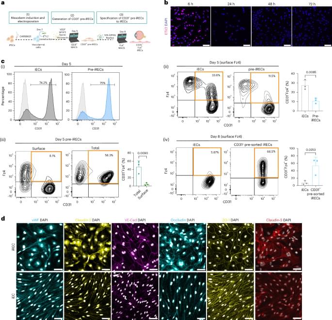
Treatment of induced pluripotent stem cells with Norrin and vitronectin, and subsequent cell sorting and maturation, generates retinal-like endothelial cells that can regenerate retinal vasculature in an oxygen-induced retinopathy mouse and recapitulate enhanced inner blood–retinal barrier properties when co-cultured with retinal-like pericytes.
“That which does not kill us only makes us stranger.”
14 years ago, I sat down with Dr. Anders Sandberg, computational neuroscientist and research fellow at Oxford’s Future of Humanity Institute, for his second appearance on my podcast. His twist on Nietzsche has stayed with me ever since.
This was 2012. Before ChatGPT, before CRISPR babies, before Neuralink implants in human skulls. And yet listen to what we covered:
The ethics of transhumanism and the limits of being human The Epic of Gilgamesh and humanity’s oldest obsession: immortality Enhancement arms-races and the risk of conflict between transhumanists and neo-luddites Hive-minds, distributed intelligence, and whether the Borg should scare us Mind uploading and what survives when the body doesn’t.
What strikes me now, rewatching it, is how little the fundamental questions have changed. The technology raced ahead. The philosophy is still catching up.
Anders argued that embracing strangeness is not a bug of the human future; it’s the feature. The question was never whether we would change. It’s whether we will change wisely.

