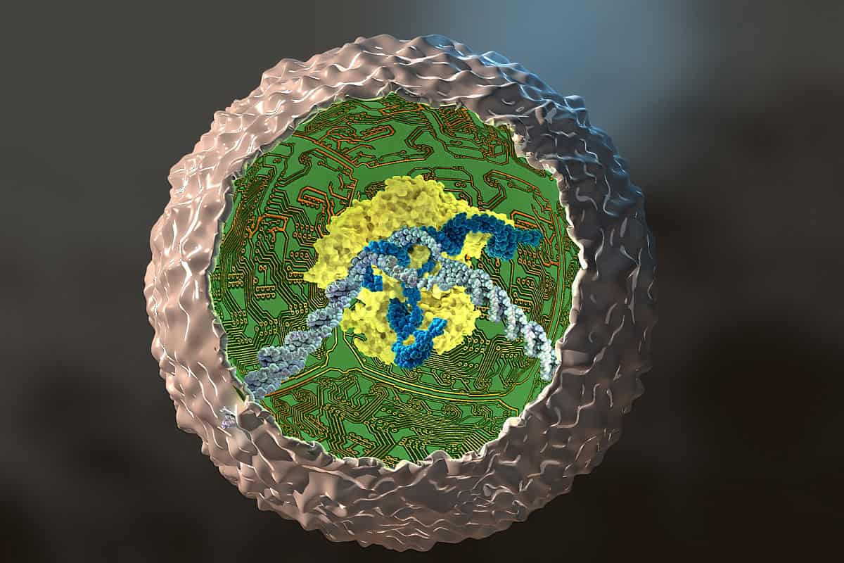
Toggle light / dark theme

Quantum metallurgy: Electron crystals deform and melt

In a process analogous to how solids melt into liquids, the electrons in many different metals form crystal-like patterns that can deform and melt, opening new pathways for neuromorphic computing and superconductors, University of Michigan Engineering researchers have found.

“Our work shows that these quantum structures, which are often thought to have a highly ordered structure, actually span a continuum of disorder that could be leveraged to engineer and control these materials,” said Robert Hovden, associate professor of materials science and engineering and corresponding author of the study published in Matter.

“Metallurgists often control defects, or disorder, in metals to produce specific properties,” Hovden said. “A similar approach might help us harness the potential of quantum materials in future devices. Quantum metallurgy could be the future.”

Focused helium ions create ferroelectric regions in aluminum nitride for lower-power chips

Scientists at the Department of Energy’s Oak Ridge National Laboratory have shown for the first time that ferroelectricity can be directly written into aluminum nitride using a tightly focused helium ion beam at the Center for Nanophase Materials Sciences (CNMS), a DOE Office of Science user facility at ORNL. Ferroelectric devices don’t need constant power to store data, which allows for devices that are more reliable and less power consuming than what’s currently available.

The study, published in Advanced Materials, represents a new processing approach for wurtzite III-V nitrides, a class of semiconductors already widely used in microelectronics but whose ferroelectric potential has only been recognized since 2019.

“Today, both the material and the processing method are already employed in chip manufacturing: aluminum nitride is widely used in many 5G and Wi-Fi devices, and helium ion beams are common tools to make tiny changes to circuits,” said Bogdan Dryzhakov, an ORNL postdoctoral research associate at CNMS.

Researchers combine five metals to build a better nanocrystal

A nanocrystal is an extraordinarily tiny piece of material—composed of anywhere from a few to a few thousand atoms—in which atoms are arranged in a precise, ordered structure. Think of it like taking a piece of gold and shrinking it down to the size of a few hundred atoms. It’s still gold, still crystalline, just almost incomprehensibly small.

Nanocrystals are in the transistors inside computers and smartphones, in smartphone displays and TV screens, in the gold-nanoparticle sensors that power COVID and pregnancy tests, and in the pipes of your car exhaust system, among countless other innovations.

Their small size gives them a dramatically higher ratio of surface area to volume, making them especially useful as catalysts—materials that speed up chemical reactions without being consumed in the process.

Quantum Entangles the Heavens

As the United States, Europe, and China compete to shape the future of the Earth-Moon corridor, strategic advantage will depend not only on launch capacity or lunar infrastructure, but also on advances in quantum technologies. Just as secure systems are critical on Earth, satellites and space-based systems underpin high-value, high-impact operations from financial transactions and navigation to scientific discovery and classified military missions.

Quantum technologies, which enable new levels of speed, sensitivity, and security, are emerging as critical tools to improve existing extraterrestrial systems. Modern digital communications are secured by encryption built on math problems that are extremely difficult for regular computers to solve, but that sufficiently advanced quantum computers could eventually crack. Quantum communications technologies could add a new layer of protection by making it easier to detect when someone is trying to intercept sensitive information. Quantum sensors can measure position and time with an accuracy that GPS only approximates. Lastly, quantum computers could unlock new capabilities beyond current computational limits, from designing advanced materials to optimizing increasingly complex satellite networks.

Countries are racing to match their space and quantum ambitions with national strategies. The White House is reportedly drafting an executive order to strengthen US competitiveness in quantum technologies. The rumored draft directs multiple US government bodies, including NASA, to develop a five-year roadmap to expand quantum sensing and networking capabilities. The EU’s 2025 Quantum Europe Strategy highlights “Space and Dual-Use Quantum Technologies” as one of its five strategic focuses, and China’s 15th Five-Year Plan has called for expanding the country’s ground-to-space quantum communications network.

Researchers discover advanced language processing in the unconscious human brain

Baylor College of Medicine researchers have found that the human brain is capable of sophisticated language processing while in an unconscious state from general anesthesia. The findings, published in the latest edition of Nature, challenge what we know about the role of consciousness and cognition, and could open new ways of understanding memory, language and brain-computer interfaces.

“Our findings show that the brain is far more active and capable during unconsciousness than previously thought,” said Dr. Sameer Sheth, professor and Cullen Foundation Endowed chair of neurosurgery and a McNair Scholar at Baylor. “Even when patients are fully anesthetized, their brains continue to analyze the world around them.”

Sheth, who is also a neurosurgeon at Baylor St. Luke’s Medical Center, and his collaborators first recorded neural activity from hundreds of individual neurons in the hippocampus, a part of the brain associated with memory, while patients were under general anesthesia during epilepsy surgery. Patients undergoing this type of surgery were sought after because it allowed researchers access to this particular part of the brain.

A persistent quantum computing error finally explained

Scientists have discovered the cause of a persistent glitch that continues to disrupt superconducting quantum computers, even when they have built-in defenses. For all their advanced hardware, superconducting quantum computers are vulnerable to errors caused by ionizing radiation from space or the environment. Radiation particles interfere with the chip substrate (the silicon base the processor is built on), which leads to the creation of rogue particles (quasiparticles) that disrupt the qubits, the basic units of quantum computers.

To protect against this, scientists developed a technique called gap engineering. This involves creating an energy barrier in the superconducting material of the qubits, making it harder for these particles to reach sensitive parts of the device.

However, it is not foolproof. Even with this defense, radiation can still cause sudden widespread errors affecting many qubits at once (error bursts). But it was not clear why.

Twisting atom-thin materials reveals new way to save computing energy

A recent study shows a new and potentially more energy-efficient way for information to be transmitted inside electronic systems, including computers and phones—without relying on electric currents or external magnetic fields.

In today’s electronics, information is transmitted by moving electrons through circuits, where ones and zeros are represented by high or low electrical signals. While this approach has enabled modern computing, the movement of electrical charge inevitably generates heat, leading to energy loss and limiting how much devices can be miniaturized and improved.

In the new study, published in Nano Letters, researchers at KTH Royal Institute of Technology and international collaborators demonstrate that simply twisting two layers of certain atom-thin magnetic materials allows magnetic signals to carry information instead of relying on electrical currents to do the work.

Researchers discover a new pathway to building energy-efficient computing chips

The growing popularity of electronic devices—from fitness trackers and laptops to smartphones—is driving demand for more energy-efficient computing chips. Now, researchers have found a way to change the electronic properties of a common semiconductor material, potentially laying the foundation for faster, lower-power data storage and processing.

In a study published in Science, a UC Berkeley-led team of researchers discovered they can transform titanium dioxide (TiO₂) into a ferroelectric material by reducing its thickness to less than 3 nanometers (nm), roughly the diameter of a single strand of human DNA. These findings, according to the researchers, could open a pathway toward ultra-scaled, energy-efficient electronic devices.

Ferroelectric materials, with their ability to switch electric polarizations, have a long history in the semiconductor industry. Today, many researchers believe that they may hold the key to enabling next-generation, energy-efficient nanoelectronics, including non-volatile memory, logic devices and emerging computing technologies.

SpaceX files for $55 billion semiconductor fab in rural Texas for Musk’s Terafab — total chipmaking fab investment could reach $119 billion

SpaceX has filed a property tax abatement application in Grimes County, Texas, for a semiconductor fab that would cost $55 billion in its initial phases and up to $119 billion if all planned expansions are completed.

The filing, posted on the county government’s website ahead of a public hearing scheduled for June 3, describes the project as a “multi-phase, next-generation, vertically integrated semiconductor manufacturing and advanced computing fabrication facility” to be built at the Gibbons Creek Reservoir site, roughly 90 miles northeast of Austin.

The capital figures in this filing far exceed what was disclosed when Elon Musk announced Terafab in March, where the project carried a $20 billion price tag. Musk later confirmed during Tesla’s earnings call that SpaceX would handle high-volume chip manufacturing while Tesla operates a smaller R&D pilot line at its Austin campus. The Grimes County filing appears to be SpaceX’s first formal step toward securing a site for that production facility.

/* */