Researchers from the Moscow Institute of Physics and Technology (MIPT) have for the first time experimentally demonstrated that copper nanophotonic components can operate successfully in photonic devices – it was previously believed that only gold and silver components could do so. Copper components are not only just as good as components based on noble metals; they can also be easily implemented in integrated circuits using industry-standard fabrication processes. “This is a kind of revolution – using copper will solve one of the main problems in nanophotonics,” say the authors of the paper. The results have been published in the scientific journal Nano Letters.
The discovery, which is revolutionary for photonics and the computers of the future, was made by researchers from the Laboratory of Nanooptics and Plasmonics at MIPT’s Centre of Nanoscale Optoelectronics. They have succeeded, for the first time, in producing copper nanophotonic components, whose characteristics are just as good as those of gold components. It is interesting to note that the scientists fabricated the copper components using the process compatible with the industry-standard manufacturing technologies that are used today to produce modern integrated circuits. This means that in the very near future copper nanophotonic components will form a basis for the development of energy-efficient light sources, ultra-sensitive sensors, as well as high-performance optoelectronic processors with several thousand cores.
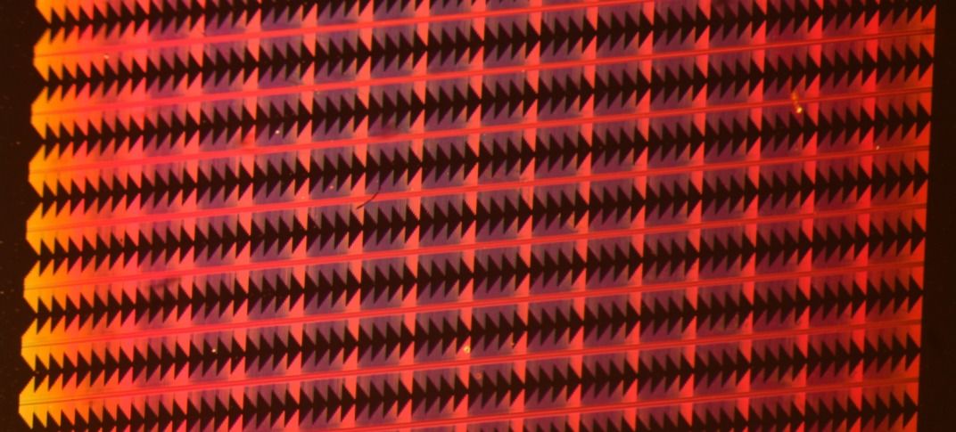
The discovery was made under what is known as nanophotonics – a branch of research which aims, among other things, to replace existing components in data processing devices with more modern components by using photons instead of electrons. However, while transistors can be scaled down in size to a few nanometres, the diffraction of light limits the minimum dimensions of photonic components to the size of about the light wavelength (~1 micrometre). Despite the fundamental nature of this so-called diffraction limit, one can overcome it by using metal-dielectric structures to create truly nanoscale photonic components. Firstly, most metals show a negative permittivity at optical frequencies, and light cannot propagate through them, penetrating to a depth of only 25 nanometres. Secondly, light may be converted into surface plasmon polaritons, surface waves propagating along the surface of a metal. This makes it possible to switch from conventional 3D photonics to 2D surface plasmon photonics, which is known as plasmonics. This offers the possibility of controlling light at a scale of around 100 nanometres, i.e., far beyond the diffraction limit.