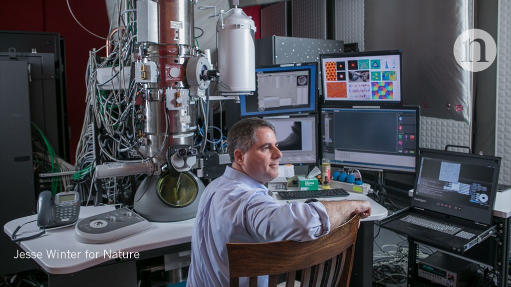
Scientists can’t study what they can’t measure — as David Muller knows only too well. An applied physicist, Muller has been grappling for years with the limitations of the best imaging tools available as he seeks to probe materials at the atomic scale.
One particularly vexing quarry has been ultra-thin layers of the material molybdenum disulfide, which show promise for building thin, flexible electronics. Muller and his colleagues at Cornell University in Ithaca, New York, have spent years peering at MoS2 samples under an electron microscope to discern their atomic structures. The problem was seeing the sulfur atoms clearly, Muller says. Raising the energy of the electron beam would sharpen the image, but knock atoms out of the MoS2 sheet in the process. Anyone hoping to say something definitive about defects in the structure would have to guess. “It would take a lot of courage, and maybe half the time, you’d be right,” he says.
This July, Muller’s team reported a breakthrough. Using an ultra-sensitive detector that the researchers had created and a special method for reconstructing the data, they resolved features in MoS2 down to 0.39 angstroms, two and a half times better than a conventional electron microscope would achieve. (1 Å is one-tenth of a nanometre, and a common measure of atomic bond lengths.) At once, formerly fuzzy sulfur atoms now showed up clearly — and so did ‘holes’ where they were absent. Ordinary electron microscopy is “like flying propeller planes”, Muller says. “Now we have a jet.”