In a new report published on Scientific Reports, Milan M. Milošević and an international research team at the Zepler Institute for Photonics and Nanoelectronics, Etaphase Incorporated and the Departments of Chemistry, Physics and Astronomy, in the U.S. and the U.K. Introduced a hyperuniform-disordered platform to realize near-infrared (NIR) photonic devices to create, detect and manipulate light. They built the device on a silicon-on-insulator (SOI) platform to demonstrate the functionality of the structures in a flexible, silicon-integrated circuit unconstrained by crystalline symmetries. The scientists reported results for passive device elements, including waveguides and resonators seamlessly integrated with conventional silicon-on-insulator strip waveguides and vertical couplers. The hyperuniform-disordered platform improved compactness and enhanced energy efficiency as well as temperature stability, compared to silicon photonic devices fabricated on rib and strip waveguides.
Academic and commercial efforts worldwide in the field of silicon photonics have led to engineer optical data communications at the Terabit-scale at increasingly lower costs to meet the rapidly growing demand in data centers. Explosive growth in cloud computing and entertainment-on-demand pose increasingly challenging costs and energy requirements for data transmission, processing and storage. Optical interconnects can replace traditional copper-based solutions to offer steadily increasing potential to minimize latency and power consumption, while maximizing the bandwidth and reliability of the devices. Silicon photonics also leverage large-scale, complementary metal-oxide semiconductor (CMOS) manufacturing processes to produce high-performance optical transceivers with high yield at low-cost. The properties allow applications of optical transceivers (fiber optical technology to send and receive data) to be increasingly compelling across shorter distances.
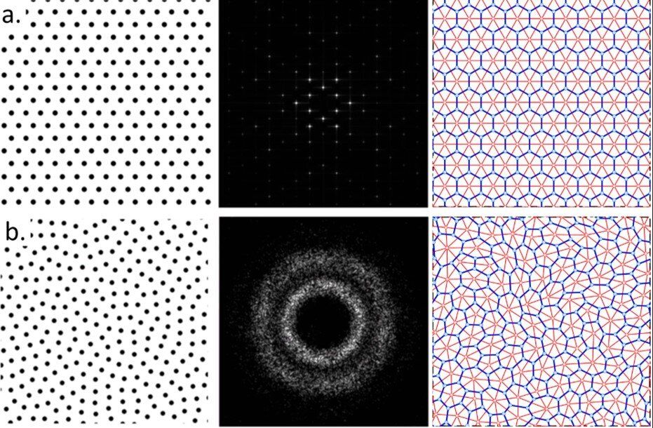
More than three decades ago, physicist Richard Soref identified silicon as a promising material for photonic integration. Leading to the present-day steady development and rapid production of increasingly complex photonic integrated circuits (PICs). Researchers can integrate large numbers of massively-parallel compact energy-efficient optical components on a single chip for cloud computing applications from deep learning to artificial intelligence and the internet of things. Compared to the limited scope of commercial silicon photonic systems, photonic crystal (PhC) architectures promise smaller device sizes, although they are withheld by layout constraints imposed by waveguide requirements along the photonic crystal’s axis. Until recently, photonic band gap (PBG) structures that efficiently guide light were limited to photonic crystal platforms. Now, newer classes of PBG structures include photonic quasicrystals, hyperuniform disordered solids (HUDs) and local self-uniform structures.