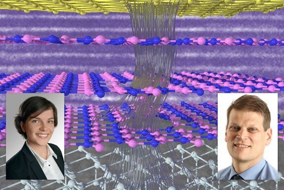
For decades, there has been a trend in microelectronics towards ever smaller and more compact transistors. 2D materials such as graphene are seen as a beacon of hope here: they are the thinnest material layers that can possibly exist, consisting of only one or a few atomic layers. Nevertheless, they can conduct electrical currents—conventional silicon technology, on the other hand, no longer works properly if the layers become too thin.
However, such materials are not used in a vacuum; they have to be combined with suitable insulators—in order to seal them off from unwanted environmental influences, and also in order to control the flow of current via the so-called field effect. Until now, hexagonal boron nitride (hBN) has frequently been used for this purpose as it forms an excellent environment for 2D materials. However, studies conducted by TU Wien, in cooperation with ETH Zurich, the Russian Ioffe Institute and researchers from Saudi Arabia and Japan, now show that, contrary to previous assumptions, thin hBN layers are not suitable as insulators for future miniaturized field-effect transistors, as exorbitant leakage currents occur. So if 2D materials are really to revolutionize the semiconductor industry, one has to start looking for other insulator materials. The study has now been published in the scientific journal Nature Electronics.