Applied Materials said it has reached a breakthrough in chip wiring that will enable semiconductor chip production to miniaturize to chips so the width between circuits can be as little as three billionths of a meter. Current chip factories are making 7nm and 5nm chips, so the 3nm chips represent the next generation of technology.
These 3nm production lines will be part of factories that cost more than $22 billion to build — and generate a lot more revenue than that. The breakthrough in chip wiring will enable logic chips to scale to three nanometers and beyond, the company said.
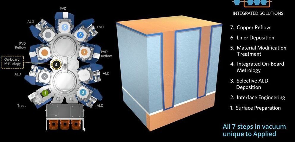
Chip manufacturing companies can use the wiring tools in their huge factories, and the transition from 5nm factories to 3nm factories could help ease a shortage of semiconductor chips that has plagued the entire electronics industry. But it will be a while before the chips go into production. In addition to interconnect scaling challenges, there are other issues related to the transistor (extending the use of FinFET transistors and transitioning to Gate All Around transistors), as well as patterning (extreme ultraviolet and multi-patterning).