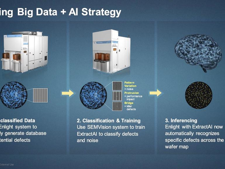
Enlight uses light polarization to maximize resolution and to find critical defects in half the time of the typical optical scanner. The scanner for the first time will capture both direct light bouncing off the wafer surface, and scattered light, known as “brightfield” and “greyfield,” respectively. That’s like scanning two things in one pass, cutting in half the time required.