“Today’s technology announcement is about challenging convention and rethinking how we continue to advance society and deliver new innovations that improve life, business and reduce our environmental impact,” said Dr. Mukesh Khare, Vice President of Hybrid Cloud and Systems, IBM Research. “Given the constraints the industry is currently facing along multiple fronts, IBM and Samsung are demonstrating our commitment to joint innovation in semiconductor design and a shared pursuit of what we call ‘hard tech.’”
Moore’s Law – an ongoing trend that shows the number of transistors on a computer chip doubling every two years or so – is now approaching what are considered fundamental barriers. Simply put, as more and more transistors are crammed into a finite area, engineers are running out of space.
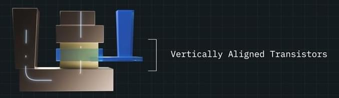
Historically, transistors have been built to lie flat upon the surface of a semiconductor, with the electric current flowing laterally, or side-to-side, through them. Vertical Transport Field Effect Transistors (VTFET), by contrast, are built perpendicular to the surface of the chip with a vertical, or up-and-down, current flow.