Hybrid bonding opens up whole new level of performance in packaging, but it’s not the only improvement.
The first wave of chips is hitting the market using a technology called hybrid bonding, setting the stage for a new and competitive era of 3D-based chip products and advanced packages.
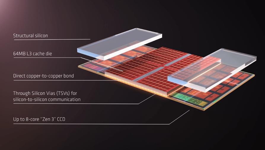
AMD is the first vendor to unveil chips using copper hybrid bonding, an advanced die-stacking technology that enables next-generation 3D-like devices and packages. Hybrid bonding stacks and connects chips using tiny copper-to-copper interconnects, providing higher density and bandwidth than existing chip-stacking interconnect schemes.