Scientists from the NTU Singapore and the Korea Institute of Machinery & Materials (KIMM) have developed a technique to create a highly uniform and scalable semiconductor wafer, paving the way to higher chip yield and more cost-efficient semiconductors.
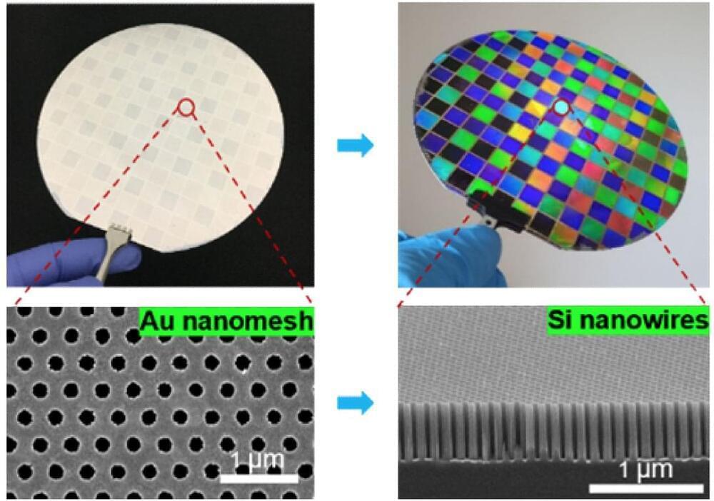
Left: Image of a six-inch silicon wafer with printed metal layers and its top-view scanning electron microscope image. Right: Image of the six-inch silicon wafer with nanowires and its cross-sectional scanning electron microscope image. (Image: NTU Singpore)
Semiconductor chips commonly found in smart phones and computers are difficult and complex to make, requiring highly advanced machines and special environments to manufacture.