Transistors are the building blocks of modern electronics, used in everything from televisions to laptops. As transistors have gotten smaller and more compact, so have electronics, which is why your cell phone is a super powerful computer that fits in the palm of your hand.
But there’s a scaling problem: Transistors are now so small that they are difficult to turn off. A key device element is the channel that charge carriers (such as electrons) travel across between electrodes. If that channel gets too short, quantum effects allow electrons to effectively jump from one side to another even when they shouldn’t.
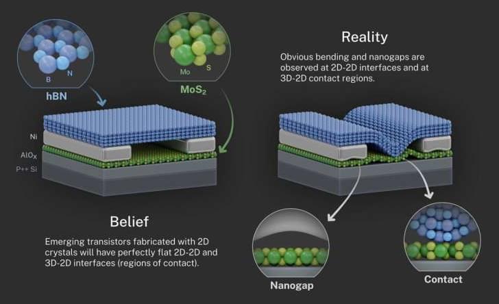
One way to get past this sizing roadblock is to use layers of 2D materials—which are only a single atom thick—as the channel. Atomically thin channels can help enable even smaller transistors by making it harder for the electrons to jump between electrodes. One well-known example of a 2D material is graphene, whose discoverers won the Nobel Prize in Physics in 2010. But there are other 2D materials, and many believe they are the future of transistors, with the promise of scaling channel thickness down from its current 3D limit of a few nanometers (nm, billionths of a meter) to less than a single nanometer thickness.