The semiconductor industry has been growing steadily ever since its first steps in the mid-twentieth century and, thanks to the high-speed information and communication technologies it enabled, it has given way to the rapid digitalization of society. Today, in line with a tight global energy demand, there is a growing need for faster, more integrated, and more energy-efficient semiconductor devices.
However, modern semiconductor processes have already reached the nanometer scale, and the design of novel high-performance materials now involves the structural analysis of semiconductor nanofilms. Reflection high-energy electron diffraction (RHEED) is a widely used analytical method for this purpose. RHEED can be used to determine the structures that form on the surface of thin films at the atomic level and can even capture structural changes in real time as the thin film is being synthesized!
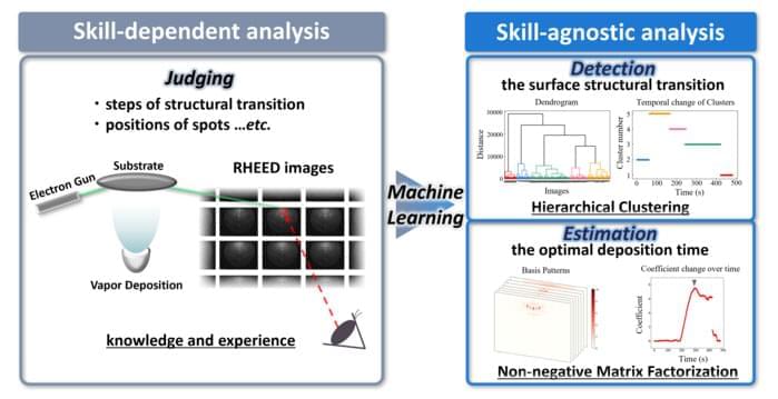
Unfortunately, for all its benefits, RHEED is sometimes hindered by the fact that its output patterns are complex and difficult to interpret. In virtually all cases, a highly skilled experimenter is needed to make sense of the huge amounts of data that RHEED can produce in the form of diffraction patterns. But what if we could make machine learning do most of the work when processing RHEED data?