The library of two-dimensional (2D) layered materials keeps growing, from basic 2D materials to metal chalcogenides. Unlike their bulk counterparts, 2D layered materials possess novel features that offer great potential in next-generation electronics and optoelectronics devices.
Doping engineering is an important and effective way to control the peculiar properties of 2D materials for the application in logical circuits, sensors, and optoelectronic devices. However, additional chemicals have to be used during the doping process, which may contaminate the materials. The techniques are only possible at specific steps during material synthesis or device fabrication.
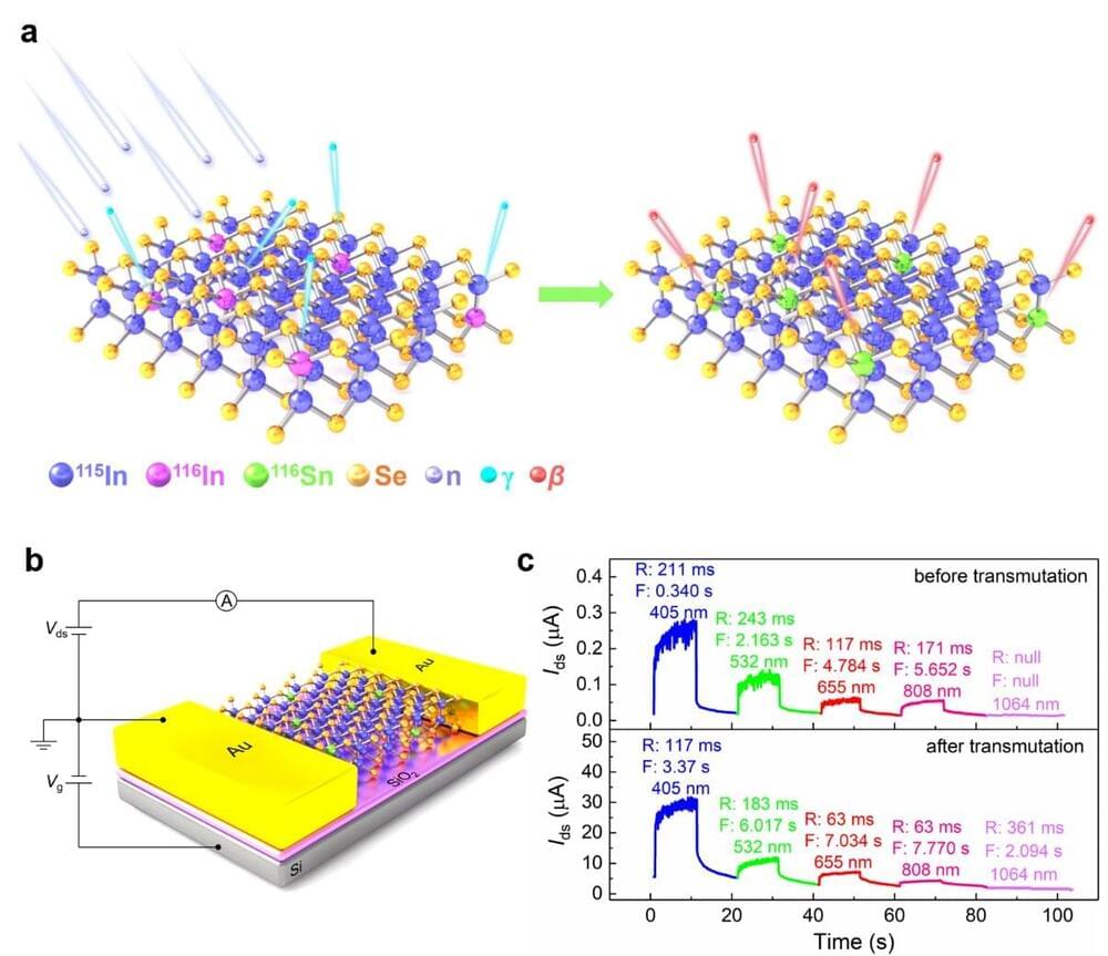
In a new paper published in eLight, a team of scientists led by Professor Han Zhang of Shenzhen University and Professor Paras N Prasad of the University of Buffalo studied the implementation of neutron-transmutation doping to manipulate electron transfer. Their paper, titled has demonstrated the change for the first time.