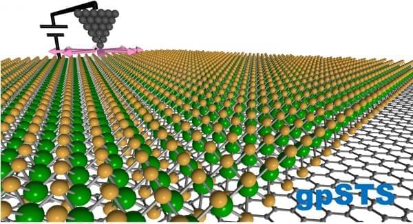
Two-dimensional materials, which consist of a single layer of atoms, exhibit unusual properties that could be harnessed for a wide range of quantum and microelectronics systems. But what makes them truly special are their flaws.
“That’s where their true magic lies,” said Alexander Weber-Bargioni at the Department of Energy’s Lawrence Berkeley National Laboratory (Berkeley Lab).
Defects down to the atomic level can influence the material’s macroscopic function and lead to novel quantum behaviors, and there are so many kinds of defects that researchers have barely begun to understand the possibilities. One of the biggest challenges in the field is systematically studying these defects at relevant scales, or with atomic resolution.