Breakthroughs in modern microelectronics depend on understanding and manipulating the movement of electrons in metal. Reducing the thickness of metal sheets to the order of nanometers can enable exquisite control over how the metal’s electrons move. By doing so, one can impart properties that aren’t seen in bulk metals, such as ultrafast conduction of electricity. Now, researchers from Osaka University and collaborating partners have synthesized a novel class of nanostructured superlattices. This study enables an unusually high degree of control over the movement of electrons within metal semiconductors, which promises to enhance the functionality of everyday technologies.
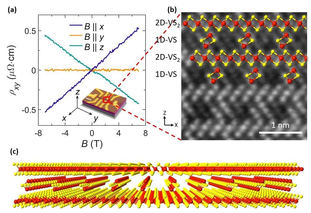
Precisely tuning the architecture of metal nanosheets, and thus facilitating advanced microelectronic functionalities, remains an ongoing line of work worldwide. In fact, several Nobel prizes have been awarded on this topic. Researchers conventionally synthesize nanostructured superlattices—regularly alternating layers of metals, sandwiched together—from materials of the same dimension; for example, sandwiched 2D sheets. A key aspect of the present researchers’ work is its facile fabrication of hetero-dimensional superlattices; for example, 1D nanoparticle chains sandwiched within 2D nanosheets.
“Nanoscale hetero-dimensional superlattices are typically challenging to prepare, but can exhibit valuable physical properties, such as anisotropic electrical conductivity,” explains Yung-Chang Lin, senior author. “We developed a versatile means of preparing such structures, and in so doing we will inspire synthesis of a wide range of custom superstructures.”