Year 2019 😁 nanoscale fusion.
A research team of fusion scientists has succeeded in developing “the nano-scale sculpture technique” to fabricate an ultra-thin film by sharpening a tungsten sample with a focused ion beam. This enables the nano-scale observation of a cross-section very near the top surface of the tungsten sample using the transmission electron microscope. The sculpture technique developed by this research can be applied not only to tungsten but also to other hard materials.
Hardened materials such as metals, carbons and ceramics are used in automobiles, aircraft and buildings. In a fusion reactor study, “tungsten,” which is one of the hardest metal materials, is the most likely candidate for the armour material of the device that receives the plasma heat/particle load. This device is called divertor. In any hardened materials, nanometer scale damages or defects can be formed very near the top surface of the materials. For predicting a material lifetime, it is necessary to know the types of the damages and their depth profiles in the material. To do this, we must observe a cross-section of the region very near the top surface of the material with nano-scale level.
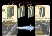
For the observation of the internal structure of materials with nano-scale level, transmission electron microscope (TEM), in which accelerated electrons are transmitted through the target materials, is commonly used as a powerful tool. In order to observe a cross-section very near the top surface of the tungsten with TEM, we firstly extract a small piece of the tungsten sample from its surface and then fabricate an ultra-thin film by cutting the extracted sample. The thickness of the film must be below ~100 nm (nanometer) to obtain high resolution due to the high-transmission of the electron beam (IMAGE 1). However, it has been extremely difficult to fabricate such an ultra-thin film for the hard materials such as a tungsten. Therefore, it has been almost impossible to obtain the ~100 nm thickness level by using conventional thin-film fabrication technique.