True to Moore’s Law, the number of transistors on a microchip has doubled every year since the 1960s. But this trajectory is predicted to soon plateau because silicon — the backbone of modern transistors — loses its electrical properties once devices made from this material dip below a certain size.
Enter 2D materials — delicate, two-dimensional sheets of perfect crystals that are as thin as a single atom. At the scale of nanometers, 2D materials can conduct electrons far more efficiently than silicon. The search for next-generation transistor materials therefore has focused on 2D materials as potential successors to silicon.
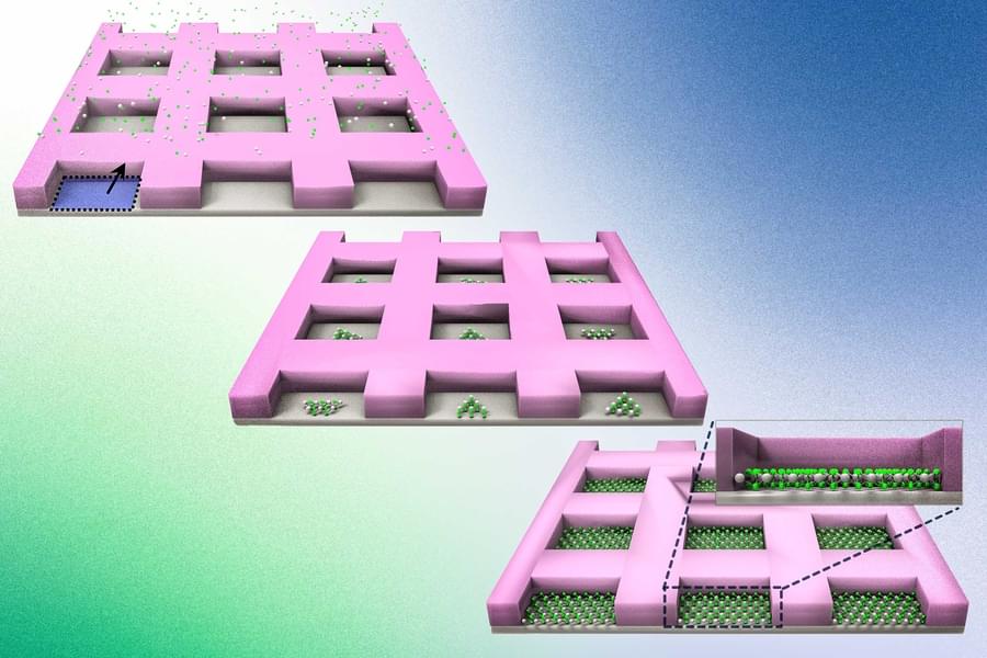
But before the electronics industry can transition to 2D materials, scientists have to first find a way to engineer the materials on industry-standard silicon wafers while preserving their perfect crystalline form. And MIT engineers may now have a solution.