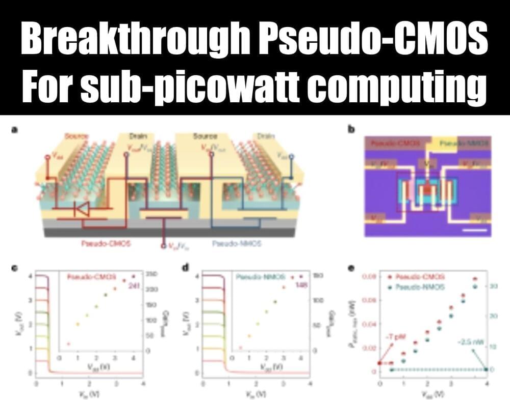
As transistors are scaled to smaller dimensions, their static power increases. Combining two-dimensional (2D) channel materials with complementary metal–oxide–semiconductor (CMOS) logic architectures could be an effective solution to this issue because of the excellent field-effect properties of 2D materials. However, 2D materials have limited polarity control. The transistors have a gapped channel that forms a tunable barrier—thus circumventing the polarity control of 2D materials—and exhibit a reverse-saturation current below 1 pA with high reliability and endurance.
They use the devices to make homojunction-loaded inverters with good rail-to-rail operation at a switching threshold voltage of around 0.5 V, a static power of a few picowatts, a dynamic delay time of around 200 µs, a noise margin of more than 90% and a peak voltage gain of 241. They also fabricate fundamental gate circuits on the basis of this pseudo-CMOS configuration by cascading several devices.