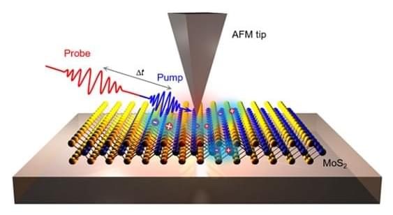
Researchers from the University of California, Berkeley have developed cutting-edge nanoscale optical imaging techniques to provide unprecedented insights into the ultrafast carrier dynamics in advanced materials. Two recent studies, published in Advanced Materials (“Transient Nanoscopy of Exciton Dynamics in 2D Transition Metal Dichalcogenides”) and ACS Photonics (“Near-Field Nanoimaging of Phases and Carrier Dynamics in Vanadium Dioxide Nanobeams”), showcase significant progress in understanding the carrier behaviors in two-dimensional and phase-change materials, with implications for next-generation electronic and optoelectronic devices.
The research team, led by Prof. Costas P. Grigoropoulos, Dr. Jingang Li, and graduate student Rundi Yang, employed a novel near-field transient nanoscopy technique to probe the behavior of materials at the nanoscale with both high spatial and temporal resolution. This approach overcomes the limitations of traditional optical methods, allowing researchers to directly visualize and analyze phenomena that were previously difficult to observe.
Schematic of the near-field transient nanoscopy. (Image: Adapted from DOI:10.1002/adma.202311568, CC BY-NC-ND 4.0)
