The dangers of AI farming.
AI could lead to new ways for people to abuse animals for financial gain. That’s why we need strong ethical guidelines.
Virginie Simoneau-Gilbert & Jonathan Birch.


Researchers report the birth of a ~2-billion-year-old orphan gene following #planetary #oxygenation, and how this humble beginning shaped the global planetary #ecosystem.
From so simple, a beginning: https://oup.silverchair-cdn.com/UI/app/svg/i.svg?versionId=192134
Abstract. Molecular innovations within key metabolisms can have profound impacts on element cycling and ecological distribution. Yet, much of the molecular foundations of early evolved enzymes and metabolisms are unknown. Here, we bring one such mystery to relief by probing the birth and evolution of the G-subunit protein, an integral component of certain members of the nitrogenase family, the only enzymes capable of biological nitrogen fixation. The G-subunit is a Paleoproterozoic-age orphan protein that appears more than 1 billion years after the origin of nitrogenases. We show that the G-subunit arose with novel nitrogenase metal dependence and the ecological expansion of nitrogen-fixing microbes following the transition in enviromental metal availabilities and atmospheric oxygenation that began ∼2.5 billion years ago. We identify molecular features that suggest early G-subunit proteins mediated cofactor or protein interactions required for novel metal dependency, priming ancient nitrogenases and their hosts to exploit these newly diversified geochemical environments. We further examined the degree of functional specialization in G-subunit evolution with extant and ancestral homologs using laboratory reconstruction experiments. Our results indicate that permanent recruitment of the orphan protein depended on the prior establishment of conserved molecular features and showcase how contingent evolutionary novelties might shape ecologically important microbial innovations.


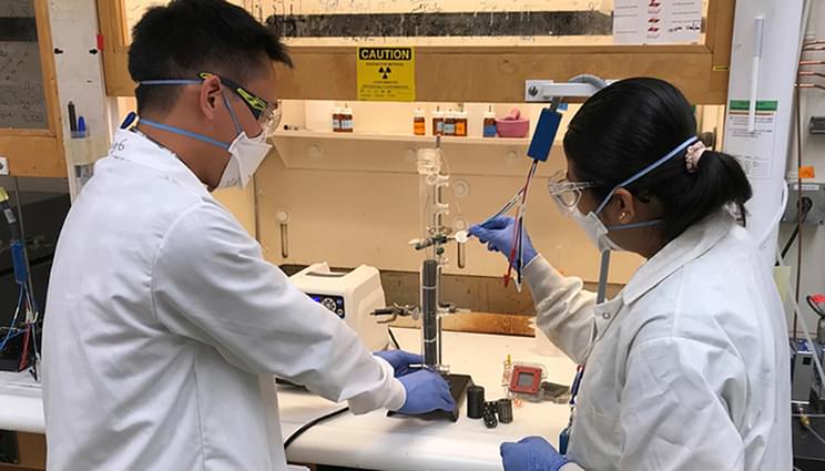
Four Lawrence Livermore National Laboratory (LLNL) researchers have partnered with Los Angeles-based SoCalGas and Munich, Germany-based Electrochaea to develop an electrobioreactor to allow excess renewable electricity from wind and solar sources to be stored in chemical bonds as renewable natural gas.
When renewable electricity supply exceeds demand, electric-utility operators intentionally curtail production of renewable electricity to avoid overloading the grid. In 2020, in California, more than 1.5 million megawatt hours of renewable electricity were curtailed, enough to power more than 100,000 households for a full year.
This practice also occurs in other countries. The team’s electrobioreactor uses the renewable electricity to convert water into hydrogen and oxygen. The microbes then use the hydrogen to convert carbon dioxide into methane, which is a major component of natural gas. Methane can then be moved around in natural gas pipelines and can be stored indefinitely, allowing the renewable energy to be recovered when it is most needed.

Probabilistic computing with stochastic devices.
In recent decades, artificial intelligence has been successively employed in the fields of finance, commerce, and other industries. However, imitating high-level brain functions, such as imagination and inference, pose several challenges as they are relevant to a particular type of noise in a biological neuron network. Probabilistic computing algorithms based on restricted Boltzmann machine and Bayesian inference that use silicon electronics have progressed significantly in terms of mimicking probabilistic inference. However, the quasi-random noise generated from additional circuits or algorithms presents a major challenge for silicon electronics to realize the true stochasticity of biological neuron systems. Artificial neurons based on emerging devices, such as memristors and ferroelectric field-effect transistors with inherent stochasticity can produce uncertain non-linear output spikes, which may be the key to make machine learning closer to the human brain. In this article, we present a comprehensive review of the recent advances in the emerging stochastic artificial neurons (SANs) in terms of probabilistic computing. We briefly introduce the biological neurons, neuron models, and silicon neurons before presenting the detailed working mechanisms of various SANs. Finally, the merits and demerits of silicon-based and emerging neurons are discussed, and the outlook for SANs is presented.
Keywords: brain-inspired computing, artificial neurons, stochastic neurons, memristive devices, stochastic electronics.

Neuromorphic computing is an emerging solution for companies specializing in small, energy-efficient edge computing devices and robotics, striving to improve their products. There has been a paradigm shift in computing since the advent of neuromorphic chips. With the potential to unlock new levels of processing speed, energy efficiency, and adaptability, neuromorphic chips are here to stay. Industries from robotics to healthcare are exploring the potential of neuromorphic chips in various applications.
What is Neuromorphic Computing?
Neuromorphic computing is a field within computer science and engineering that draws inspiration from the structure and operation of the human brain. Its goal is to create computational systems, including custom hardware replicating the neural networks and synapses in biological brains. These custom computational systems are commonly known as neuromorphic chips or neuromorphic hardware.
In cells, like the snowflake yeast in this image byTony Burnetti, proteins are translated and folded into very specific, three-dimensional shapes. | Cell And Molecular Biology.


In a recent study published in Nature Communications, researchers developed a modular synthetic biology toolkit for Aspergillus oryzae, an edible fungus used in fermented foods, protein production, and meat alternatives.
Study: Edible mycelium bioengineered for enhanced nutritional value and sensory appeal using a modular synthetic biology toolkit. Image Credit: Rattiya Thongdumhyu/Shutterstock.com.
Join us on Patreon! https://www.patreon.com/MichaelLustgartenPhDDiscount Links: Epigenetic, Telomere Testing: https://trudiagnostic.com/?irclickid=U-s3Ii2r7x…