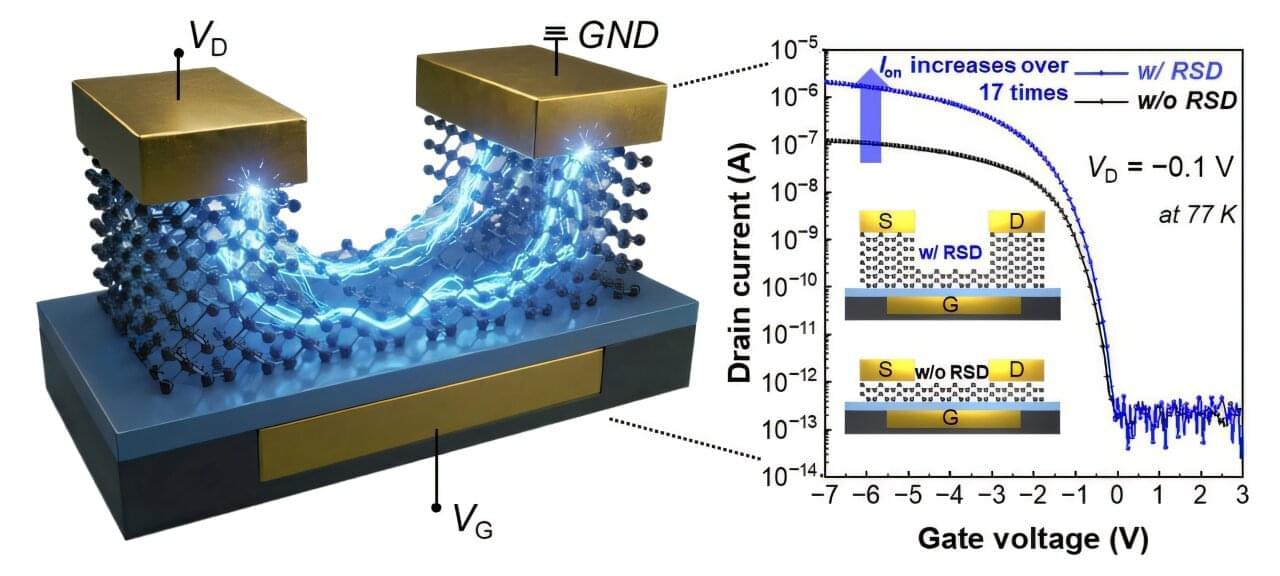
Toggle light / dark theme

‘Like talking on the telephone’: Quantum computing engineers get atoms chatting long distance

UNSW engineers have made a significant advance in quantum computing: they created ‘quantum entangled states’—where two separate particles become so deeply linked they no longer behave independently—using the spins of two atomic nuclei. Such states of entanglement are the key resource that gives quantum computers their edge over conventional ones.

The research is published in the journal Science, and is an important step toward building large-scale quantum computers—one of the most exciting scientific and technological challenges of the 21st century.

Lead author Dr. Holly Stemp says the achievement unlocks the potential to build the future microchips needed for quantum computing using existing technology and manufacturing processes.

How you make it matters: Spintronics device performance tied to atomic interface changes

Spintronics devices will be key to realizing faster and more energy-efficient computers. To give us a better understanding of how to make them, a Kobe University team now showed how different manufacturing techniques influence the material properties of a key component.

Electronic devices could be made more efficient and faster if electrons could carry more information at once. This is the basic idea behind spintronics, where researchers try to use the electrons’ spin in addition to charge in , processing and sensor devices to significantly improve our computers.

One component for such devices is the “,” which may be used, for example, for neuron-like behavior in information processing or in a new type of fast and non-volatile memory. They consist of two ferromagnets, usually a nickel-iron alloy, sandwiching a thin insulating layer such as graphene.

Universal scheme efficiently generates arbitrary two-qubit gates in superconducting quantum processors

The operation of quantum computers, systems that process information leveraging quantum mechanical effects, relies on the implementation of quantum logic gates. These are essentially operations that manipulate qubits, units of information that can exist in a superposition of states and can become entangled.

A type of quantum logic gate that enables the entanglement between is a so-called two-qubit gate. Notably, most existing schemes for generating these gates force qubits outside of the conditions or parameters in which they can best store information and are easier to control.

Researchers at the Beijing Academy of Quantum Information Sciences (BAQIS) and Tsinghua University recently introduced a new universal scheme to implement two-qubit gates in superconducting quantum processors. This scheme, outlined in a paper published in Nature Physics, was found to reliably enable the generation of entanglement between qubits in superconductor-based quantum computers.

If quantum computing is answering unknowable questions, how do we know they’re right?

Quantum computing promises to solve the seemingly unsolvable in fields such as physics, medicine, cryptography and more.

But as the race to develop the first large-scale, error-free commercial device heats up, it begs the question: how can we check that these ‘impossible’ solutions are correct?

A new Swinburne study is tackling this paradox. The paper is published in the journal Quantum Science and Technology.

World-first quantum computer made with standard laptop chips launched

A UK startup has made a revolutionary advancement after delivering the world’s first full-stack quantum computer, built using the same silicon chip technology found in smartphones and laptops.

London-based Quantum Motion, a quantum computing startup that develops scalable quantum computing tech using silicon, launched the industry’s first full-stack quantum computer made with silicon. It was deployed at the UK National Quantum Computing Centre (NQCC).

Scalable strategy produces high-quality black phosphorus nanoribbons for electronics

Black phosphorus nanoribbons (BPNRs), thin and narrow ribbon-like strips of black phosphorus, are known to exhibit highly advantageous electronic properties, including a tunable bandgap. This essentially means that the energy difference between the region where electrons are bound together (i.e., valence band) and that where electrons move freely (i.e., conduction band) can be easily controlled by adjusting the width of the nanoribbons.

A tunable bandgap is essential for the development of transistors, the components that control the flow of electrical current through electronic devices.

While several past studies have highlighted the promise of BPNRs for the development of electronics, strategies that could enable their reliable fabrication on a large scale are still lacking.

Single device amplifies signals while shielding qubits from unwanted noise

Quantum computing, an approach to deriving information that leverages quantum mechanical effects, relies on qubits, quantum units of information that can exist in superpositions of states. To effectively perform quantum computing, engineers and physicists need to be able to measure the state of qubits efficiently.

In quantum computers based on , qubits are indirectly measured by a so-called readout resonator, a circuit that responds differently based on the state of a . This circuit’s responses are probed using a weak electromagnetic wave, which needs to be amplified to enable its detection.

To amplify these signals, also known as microwave tones, quantum technology engineers rely on devices known as amplifiers. Existing amplifiers, however, have notable limitations. Conventional amplifiers can send unwanted noise back to the qubit, disturbing its state. Superconducting parametric amplifiers introduced more recently can be very efficient, but they conventionally rely on bulky and magnetic hardware components that control the direction of signal and protect qubits from backaction noise.

A biocompatible and stretchable transistor for implantable devices

Recent technological advances have opened new possibilities for the development of advanced biomedical devices that could be implanted inside the human body. These devices could be used to monitor biological signals that offer insight about the evolution of specific medical conditions or could even help to alter problematic physiological processes.

Despite their potential for the diagnosis and treatment of some conditions, most developed to date are based on rigid electronic components. These components can damage tissue inside the body or cause inflammation.

Some have been trying to develop alternative implantable electronics that are based on soft and stretchable materials, such as polymers. However, most known polymers and elastic materials are not biocompatible, which means that they can provoke immune responses and adversely affect the growth of cells.

Soft ‘NeuroWorm’ electrode allows wireless repositioning and stable neural monitoring

In brain-computer interfaces (BCIs) and other neural implant systems, electrodes serve as the critical interface and are core sensors linking electronic devices with biological nervous systems. Most currently implanted electrodes are static: Once positioned, they remain fixed, sampling neural activity from only a limited region. Over time, they often elicit immune responses, suffer signal degradation, or fail entirely, which has hindered the broader application and transformative potential of BCIs.

In a study published in Nature, a team led by Prof. Liu Zhiyuan, Prof. Xu Tiantian and Assoc. Prof. Han Fei from the Shenzhen Institute of Advanced Technology of the Chinese Academy of Sciences, along with Prof. Yan Wei from Donghua University, have reported a soft, movable, long-term implantable fiber electrode called “NeuroWorm,” marking a radical shift for bioelectronic interfaces from static operation to dynamic operation and from passive recording to active, intelligent exploration.

The design of NeuroWorm is inspired by the earthworm’s flexible locomotion and segmented sensory system. By employing sophisticated electrode patterning and a rolling technique, the researchers transformed a two-dimensional array on an ultrathin flexible polymer into a tiny fiber approximately 200 micrometers in diameter.

Material that listens: Chip-based approach enables speech recognition and more

Speech recognition without heavy software or energy-hungry processors: researchers at the University of Twente, together with IBM Research Europe and Toyota Motor Europe, present a completely new approach. Their chips allow the material itself to “listen.” The publication by Prof. Wilfred van der Wiel and colleagues appears today in Nature.

Until now, has relied on cloud servers and complex software. The Twente researchers show that it can be done differently. They combined a Reconfigurable Nonlinear Processing Unit (RNPU), developed at the University of Twente, with a new IBM chip. Together, these devices process sound as smoothly and dynamically as the human ear and brain. In tests, this approach proved at least as accurate as the best software models—and sometimes even better.

The potential impact is considerable: hearing aids that use almost no energy, that no longer send data to the cloud, or cars with direct speech control. “This is a new way of thinking about intelligence in hardware,” says Prof. Van der Wiel. “We show that the material itself can be trained to listen.”

/* */