Toggle light / dark theme

Neuromorphic computing is about mimicking the human brain’s structure to deliver more efficient data processing, including faster speeds and higher accuracy, and it’s a hot topic right now. A lot of universities and tech firms are working on it, including scientists at Intel who have built the world’s largest “brain-based” computing system for Sandia National Laboratories in New Mexico.

Intel’s creation, called Hala Point, is only the size of a microwave, but boasts 1.15 billion artificial neurons. That’s a massive step up from the 50 million neuron capacity of its predecessor, Pohoiki Springs, which debuted four years ago. There’s a theme with Intel’s naming in case you were wondering – they’re locations in Hawaii.

For this technique to work at very high fidelity, a very fast and very sensitive bolometer is needed to measure the quantum state before it decays. In 2020, the Finnish researchers unveiled a bolometer that used graphene as its absorber – a fast and sensitive design that was intended for use in quantum computing. Unfortunately, this bolometer degraded over time and the team instead used an older bolometer design involving interfaces between superconductors and normal metals.

Möttönen says that the researchers had initially not expected the older design to be effective for reading out the states of individual qubits. He also expects that the read-out fidelity could be boosted using improved graphene bolometers. “I’m hoping to get the new graphene bolometers out of the oven soon,” he says.

David Pahl at the Massachusetts Institute of Technology believes that the work is very preliminary, but potentially very important. He says that the two most important performance metrics for a scheme to read out quantum states are the fidelity and the speed: “The state of the art speed that we’ve seen in the past year is 0.1 μs and 99.5% fidelity…[Möttönen and colleagues] showed 14 μs and 61.7%,” he says.

Washington University in St. Louis scientists have developed a novel material that supercharges innovation in electrostatic energy storage. The material is built from artificial heterostructures made of freestanding 2D and 3D membranes that have an energy density up to 19 times higher than commercially available capacitors.

Electrostatic capacitors play a crucial role in modern electronics. They enable ultrafast charging and discharging, providing energy storage and power for devices ranging from smartphones, laptops, and routers to medical devices, automotive electronics and industrial equipment. However, the ferroelectric materials used in capacitors have significant energy loss due to their material properties, making it difficult to provide high energy storage capability.

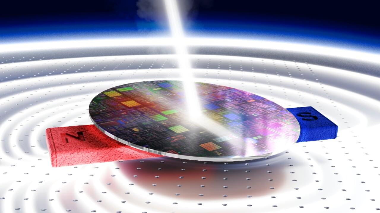
The potential of quantum technology is huge but is today largely limited to the extremely cold environments of laboratories. Now, researchers at Stockholm University, at the Nordic Institute for Theoretical Physics and at the Ca’ Foscari University of Venice have succeeded in demonstrating for the very first time how laser light can induce quantum behavior at room temperature — and make non-magnetic materials magnetic. The breakthrough is expected to pave the way for faster and more energy-efficient computers, information transfer and data storage.

Within a few decades, the advancement of quantum technology is expected to revolutionize several of society’s most important areas and pave the way for completely new technological possibilities in communication and energy.

Of particular interest for researchers in the field are the peculiar and bizarre properties of quantum particles — which deviate completely from the laws of classical physics and can make materials magnetic or superconducting.

The dynamic characteristics of the inverters have been simulated by varying the inverter output (load) capacitance (COUT), connected to the inverter output across a 1000 nm long interconnect (assumed for simulations of the NM circuit, described in “NM circuit” subsection), from 1 aF to 1 fF. By evaluating the delay \(({t}_{{{{{{\rm{p}}}}}}})\) of the input-to-outpution, and the instantaneous current drawn from the supply during thision, the average power dissipation, and the energy-delay-product (EDP), is evaluated for both the 2D-TFET and the FinFET implementations. The higher delay of the 2D-TFET (due to its lower ON-current) translates to higher EDP, and the EDP metrics get worse as the load capacitance is further increased. In fact, as will be shown later, the main advantages of TFETs are in implementations of sparse switching circuits where its much lower OFF-current and small SS help in lowering the static power dissipation, thereby improving the overall performance.

Figure 2c shows an 11-stage ring oscillator, implemented considering both interconnect and device parasitics, and designed with minimum sized 2D-TFET and FinFET inverters. Figure 2 d, e compares the transient characteristics of the FinFET and the 2D-TFET ring oscillators, from which the frequency of oscillation is extracted to be 10 GHz and 57 MHz, respectively, corresponding to single-stage delays of 10 ps and 1.6 ns. The delay of the 2D-TFET ring oscillator is larger due to its lower ON-current. The effect of the enhanced Miller capacitance in creating large overshoots and undershoots of the output voltage in TFETs is also observed in Fig. 2e.

Static random-access memory (SRAMs), which occupy up to 70% of the processor area are the main memory elements in designing CPU cache memory offering fast memory access and can be used for synapse weight retention in a designed NM system comprising of several neurons. However, this large prevalence of SRAMs also results in a large power consumption. In fact, SRAM data access in Intel’s Loihi5 has been estimated to be more energy intensive than each neuronal spike, necessitating the development of low-power SRAM implementations. Although SRAM design with 2D-TFETs can improve the energy-efficiency, the standard SRAM design utilizes two access transistors for operation, which require bidirectional current flow, and are therefore, ill-suited for implementation with unidirectional-TFETs. This necessitates the development of a modified SRAM design, which either uses a pass transistor network of TFETs, or solitary 2D-FETs, for implementing the function of the access transistors (Fig. 2f–l).

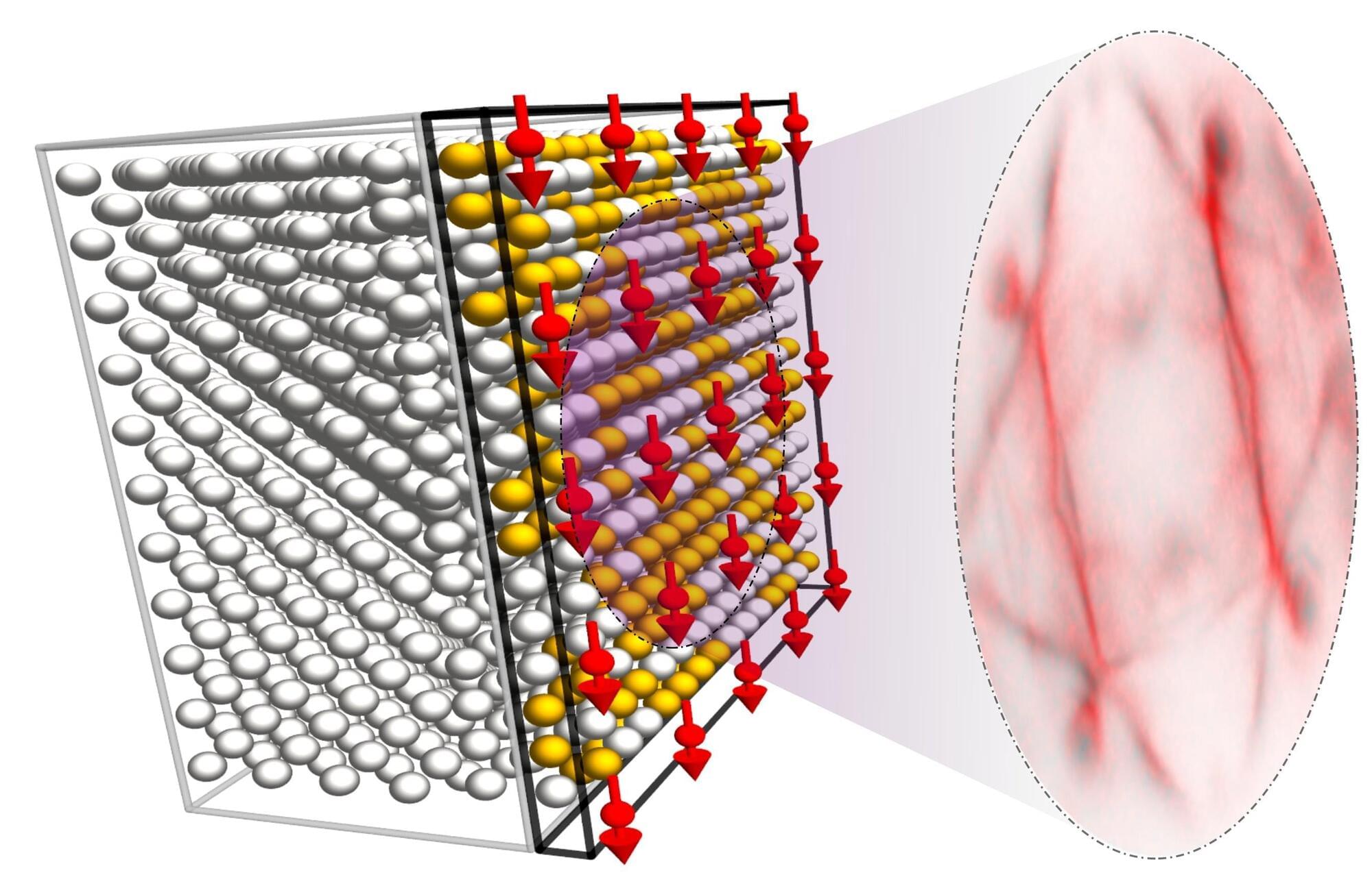
Researchers Kazuaki Takasan and Kyogo Kawaguchi of the University of Tokyo with Kyosuke Adachi of RIKEN, Japan, have demonstrated that ferromagnetism, an ordered state of atoms, can be induced by increasing particle motility and that repulsive forces between atoms are sufficient to maintain it.

The discovery not only extends the concept of active matter to but also contributes to the development of novel technologies that rely on the magnetic properties of particles, such as magnetic memory and quantum computing. The findings were published in the journal Physical Review Research.

Flocking birds, swarming bacteria, cellular flows. These are all examples of active matter, a state in which individual agents, such as birds, bacteria, or cells, self-organize. The agents change from a disordered to an ordered state in what is called a “phase transition.” As a result, they move together in an organized fashion without an external controller.

Abstract. In recent years, brain research has indisputably entered a new epoch, driven by substantial methodological advances and digitally enabled data integration and modelling at multiple scales—from molecules to the whole brain. Major advances are emerging at the intersection of neuroscience with technology and computing. This new science of the brain combines high-quality research, data integration across multiple scales, a new culture of multidisciplinary large-scale collaboration, and translation into applications. As pioneered in Europe’s Human Brain Project (HBP), a systematic approach will be essential for meeting the coming decade’s pressing medical and technological challenges.