Droplet interface bilayer was formed between two aqueous droplets immersed in hexadecane oil and lined with a lipid monolayer using the “lipid in” technique. First, to prepare the ~100-nm-diameter DPhPC large unilamellar vesicles (LUVs), 2 mg of DPhPC lipids dissolved in chloroform was placed into a glass vial. For different bilayer compositions, the total amount of DPhPC, cholesterol, and SM was kept at 2 mg while varying their mass ratios. The solvent was evaporated under an air stream and further dried overnight in a vacuum desiccator. Then, 1 ml of buffer was added to the desiccated lipid film to achieve a final lipid concentration of 2 mg/ml after a 30-s bath sonication. Unless otherwise noted, the buffer solutions in the droplets were 100 mM KCl, 10 mM tris, and 1 mM EDTA at pH 7.5. The mixtures were incubated at ambient temperature for 30 min. To form unilamellar vesicles, the samples underwent 7 freeze-thaw cycles, involving rapid freezing in liquid nitrogen and subsequent thawing at 50°C. The samples were then extruded through 100-nm pore-sized polycarbonate membranes 21 times using a mini-extruder (Avanti Polar Lipids).
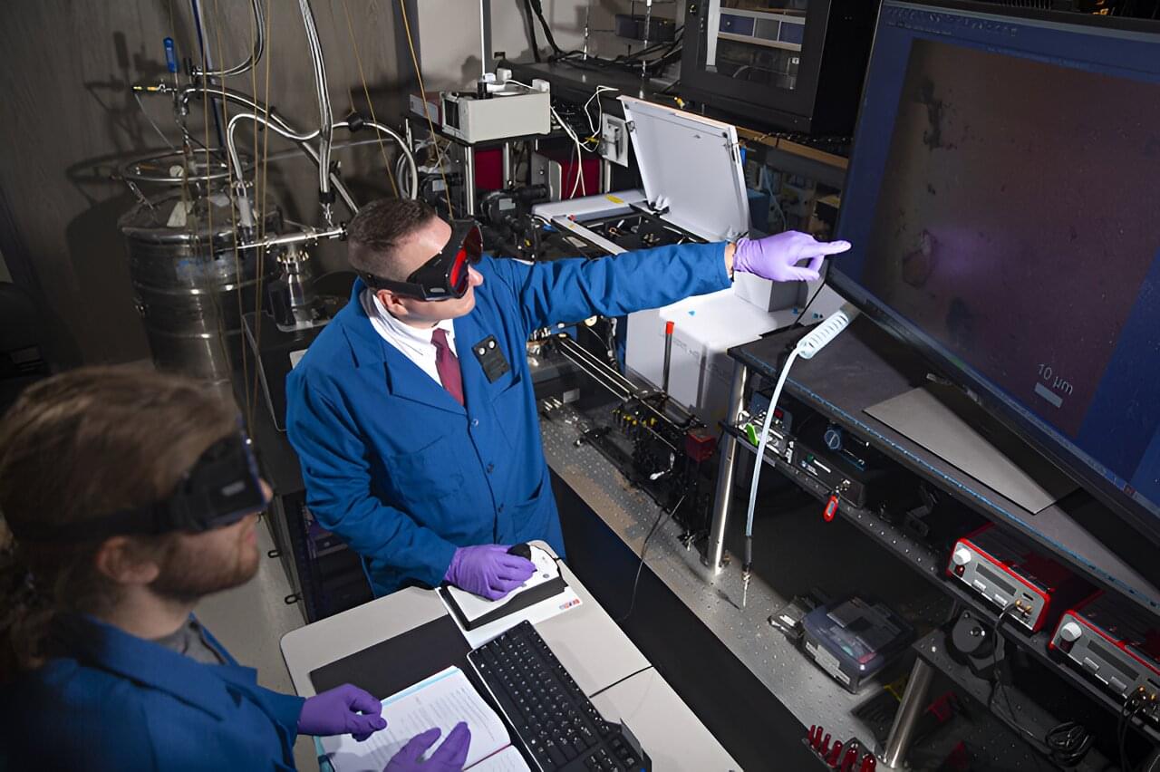
Next, two 100-μm-diameter Ag/AgCl electrodes with ball-ended tips were made hydrophilic by coating with low-melt agarose in KCl buffer (3%, w/v). The electrodes were affixed to micromanipulators (NMN-21, Narishige) mounted onto an inverted optical microscope (Leica DMi1) and connected to a patch-clamp amplifier headstage input and ground. Approximately 600-nl droplets of LUV solution were carefully placed on the electrodes in the hexadecane oil bath using a micropipette. For reconstitution of α-HL in the bilayer, a diluted α-HL stock solution (0.5 mg/ml reduced to 1 μg/ml) was added to the LUV solution before droplet formation.
The droplets were incubated for at least 5 min to allow the formation of a self-assembled lipid monolayer. During this process, the droplets sagged slightly away from the electrode, becoming relatively free from strong electrode adhesion. Subsequently, the droplets were gently brought together to form a bilayer at the interface, which was confirmed by optical microscopy imaging and membrane capacitance measurements under an applied triangular voltage wave. The relative freedom of the droplets from the electrode ensures that the electrode-droplet interfaces do not interfere with the bilayer geometry or its structural response under the applied voltages (movie S1).

