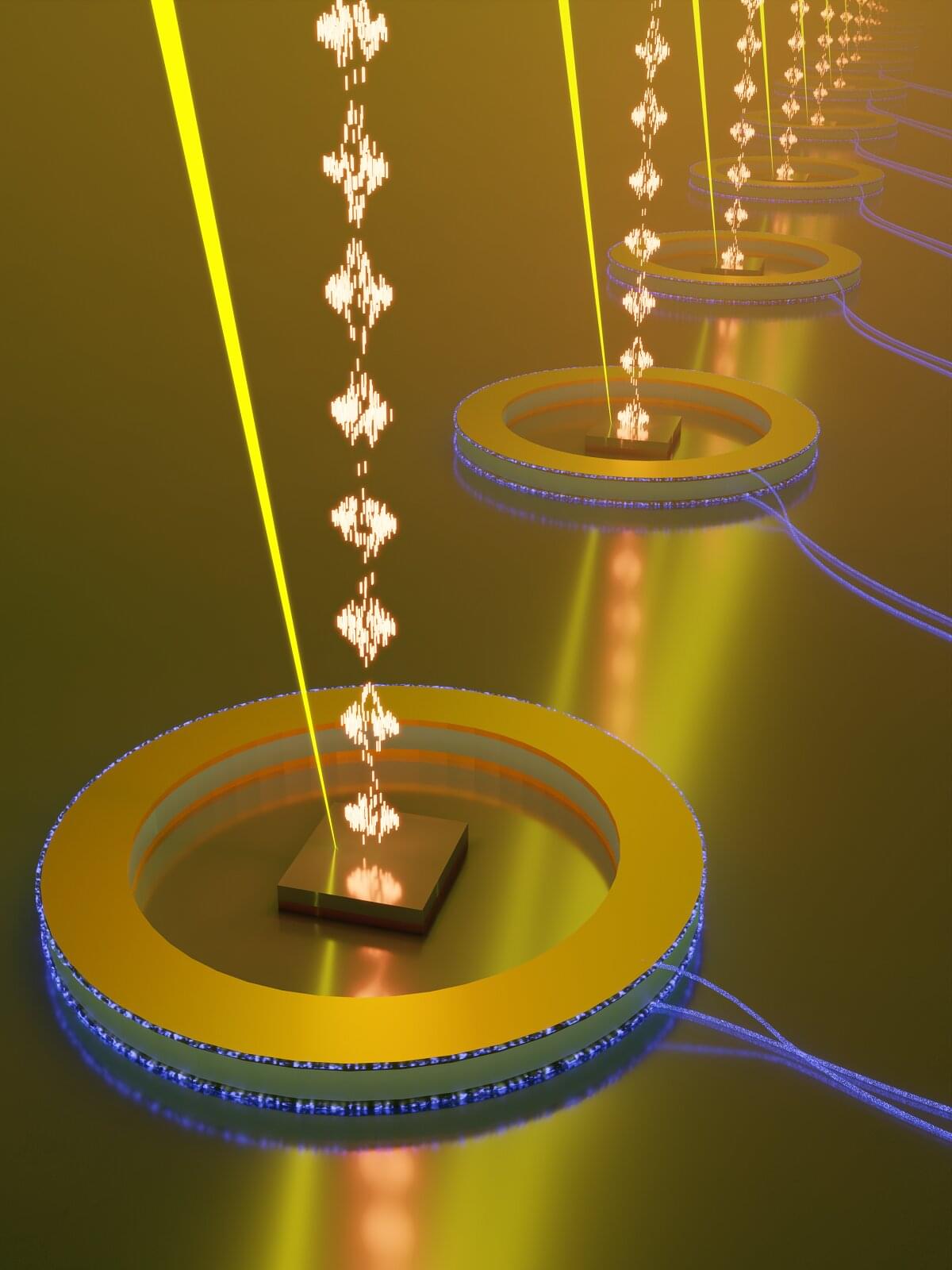
Researchers at the Harvard John A. Paulson School of Engineering and Applied Sciences (SEAS) have created a chip-scale device that can dynamically control the “handedness” of light as it passes through—also known as its optical chirality—with a simple twist of two specially designed photonic crystals. The study is published in the journal Optica.
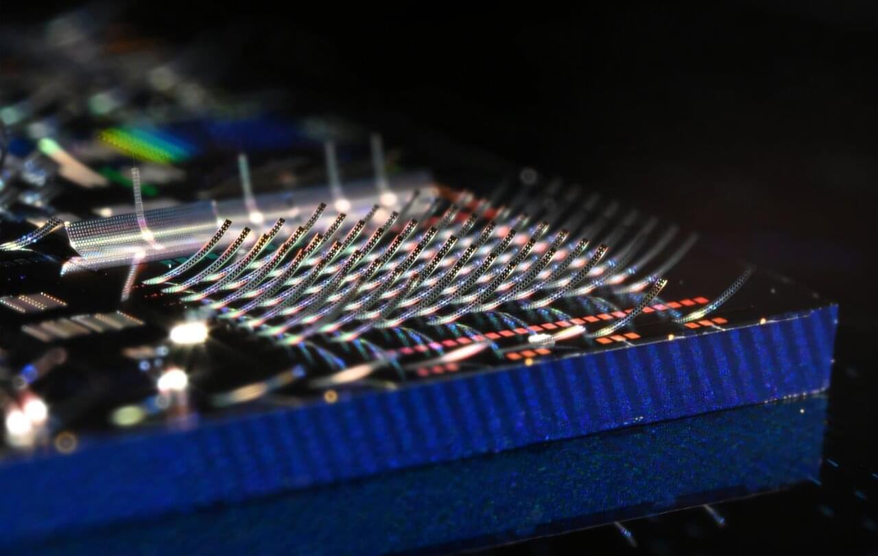
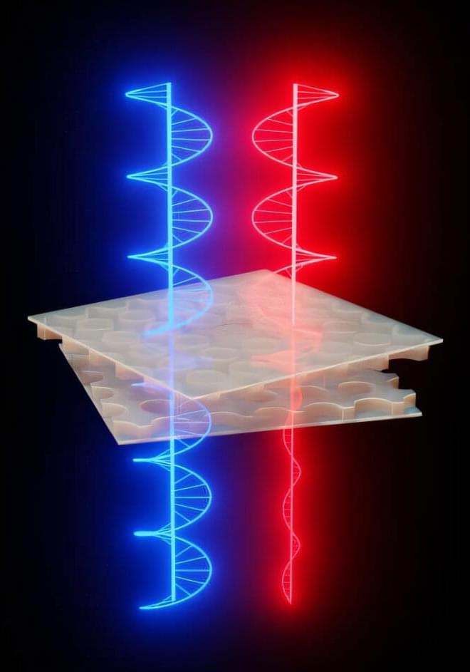
The work, led by graduate student Fan Du in the lab of Eric Mazur, the Balkanski Professor of Physics and Applied Physics, describes a reconfigurable twisted bilayer photonic crystal that can be tuned in real time using an integrated micro-electromechanical system (MEMS). The breakthrough opens new possibilities for advanced chiral sensing, optical communication, and quantum photonics.
“Chirality is very important in many fields of science—from pharma to chemistry, biology, and of course, physics and photonics,” Mazur said. “By integrating twisted photonic crystals with MEMS, we have a platform that is not only powerful from a physics standpoint, but also compatible with the way modern photonics are manufactured.”