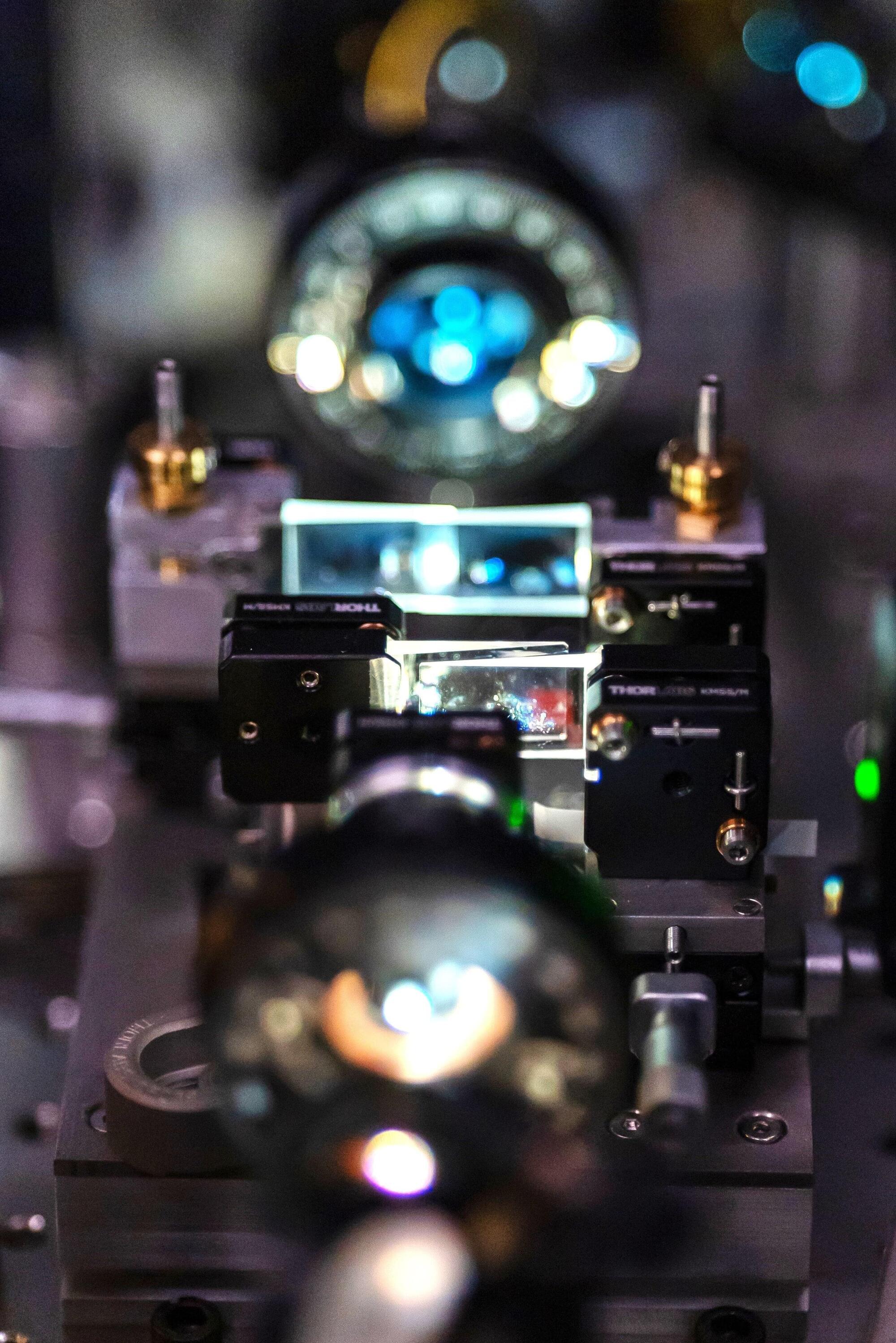
So, what an international team of scientists from Sweden and Germany have done is create hydrogels that can be controlled with electricity. This means they can easily connect them to electronic devices like computers and smartphones.
Category: computing – Page 219
Lasers are essential tools for observing, detecting, and measuring things in the natural world that we can’t see with the naked eye. But the ability to perform these tasks is often restricted by the need to use expensive and large instruments.
In a newly published cover-story paper in the journal Science, researcher Qiushi Guo demonstrates a novel approach for creating high-performance ultrafast lasers on nanophotonic chips. His work centers on miniaturizing mode-lock lasers—a unique laser that emits a train of ultrashort, coherent light pulses in femtosecond intervals, which is an astonishing quadrillionth of a second.
Ultrafast mode-locked lasers are indispensable to unlocking the secrets of the fastest timescales in nature, such as the making or breaking of molecular bonds during chemical reactions, or light propagation in a turbulent medium. The high-speed, pulse-peak intensity and broad-spectrum coverage of mode-locked lasers have also enabled numerous photonics technologies, including optical atomic clocks, biological imaging, and computers that use light to calculate and process data.
Elon Musk’s Neuralink is looking for a volunteer for its first clinical trial of a brain implant chip. The trial, which begins next year, has attracted thousands of prospective patients. The ideal candidate must be an adult under 40 with all four limbs paralyzed. The procedure involves inserting electrodes and wires into the brain, with a small computer replacing part of the skull. The computer will collect and analyze brain activity, sending the data wirelessly to a nearby device. Neuralink aims to translate thoughts into computer commands. However, the company has faced criticism for animal testing practices.
The FDA approved human trials after initially rejecting them in 2022, citing safety concerns.
The FDA had initially rejected the company’s request to run human trials back in 2022, citing safety concerns.
Magnetic random-access memories (MRAMs) are data storage devices that store digital data within nanomagnets, representing it in binary code (i.e., as “0” or “1”). The magnetization of nanomagnets inside these memory devices can be directed upward or downward.
Over the past decade, electronics engineers have introduced techniques that can switch this direction using in-plane electrical currents. These techniques ultimately enabled the creation of a new class of MRAM devices, referred to as spin-orbit torque (SOT)-MRAMs.
While existing techniques to switch magnetization direction of nanomagnets in SOT-MRAMs have proved effective, many only work if external magnetic fields are aligned with the direction of the electric current. In a recent paper published in Nature Electronics, researchers at the National University of Singapore demonstrated the field-free switching of the perpendicular magnetic anisotropy (PMA) ferromagnet cobalt iron boron (CoFeB) at ambient conditions.
Whether talking about the office kitchen, hiking trails or ratings on Yelp, there are always people who put in effort to leave those spaces better. There are also those who contribute nothing to that public good.
New research using large-scale online experiments suggests that rewarding people to contribute to a virtual public good, such as a simulated online rating for a ferry system, increased the accuracy of the ratings and improved the overall quality of that resource.
The multidisciplinary team, including researchers from the University of California, Davis; Hunter College, College of New York; the Max Planck Institute for Empirical Aesthetics; and Princeton University tested ideas about collective action in a simulation incorporating more than 500 people worldwide. Team expertise included communication science, sociology, computer science, psychology and animal behavior.
For more than 50 years, the semiconductor industry has been hard at work developing advanced technologies that have led to the amazing increases in computing power and energy efficiency that have improved our lives. A primary way the industry has achieved these remarkable performance gains has been by finding ways to decrease the size of the semiconductor devices in microchips. However, with semiconductor feature sizes now approaching only a few nanometers—just a few hundred atoms—it has become increasingly challenging to sustain continued device miniaturization.
To address the challenges associated with fabricating even smaller microchip components, the semiconductor industry is currently transitioning to a more powerful fabrication method—extreme ultraviolet (EUV) lithography. EUV lithography employs light that is only 13.5 nanometers in wavelength to form tiny circuit patterns in a photoresist, the light-sensitive material integral to the lithography process.
The photoresist is the template for forming the nanoscale circuit patterns in the silicon semiconductor. As EUV lithography begins paving the way for the future, scientists are faced with the hurdle of identifying the most effective resist materials for this new era of nanofabrication.
When you think of empty space, you almost certainly imagine a vacuum in which nothing interesting can ever happen. However, if we zoom in to tiny length scales where quantum effects start to become important, it turns out that what you thought was empty is actually filled at all times with a seething mass of electromagnetic activity, as virtual photons flicker in and out of existence. This unexpected phenomenon is known as the vacuum fluctuation field. However, because these fluctuations of light energy are so small and fleeting in time, it is difficult to find ways for matter to interact with them, especially within a single, integrated device.
In a study published this month in Nano Letters (“Electrical Detection of Ultrastrong Coherent Interaction between Terahertz Fields and Electrons Using Quantum Point Contacts”), researchers from the Institute of Industrial Science, The University of Tokyo succeeded in fabricating a single nanoscale hybrid system for doing exactly this. In their design, a quantum point contact connects a single on-chip split-ring resonator with a two-dimensional electron system.
Quantum Hall edge channels at the quantum point contact. (Image: University of Tokyo)
A new theoretical approach allows the alteration of α-RuCl3’s magnetic properties through quantum fluctuations in an optical cavity, providing a laser-free avenue for material manipulation.
Researchers in Germany and the USA have produced the first theoretical demonstration that the magnetic state of an atomically thin material, α-RuCl3, can be controlled solely by placing it into an optical cavity. Crucially, the cavity vacuum fluctuations alone are sufficient to change the material’s magnetic order from a zigzag antiferromagnet into a ferromagnet. The team’s work has been published in the scientific journal npj Computational Materials.
Advancements in Material Physics.
The widespread use of electronic devices to interact with others and access the internet has increased the need for highly performing communication technologies that can transmit data faster and more efficiently. Increasing the data transmission rate of devices without adversely impacting their energy efficiency, however, is a challenging task.
Researchers at University of Southampton in the UK recently developed a promising new transmitter based on complementary metal-oxide-semiconductor (CMOS) technology and silicon photonics. This transmitter, introduced in Nature Electronics, was found to achieve remarkable data transmission rates while consuming minimal energy.
“The integration of silicon photonics with electronics is essential for producing practical systems for numerous applications,” David J. Thomson, one of the authors of the paper, told Tech Xplore.