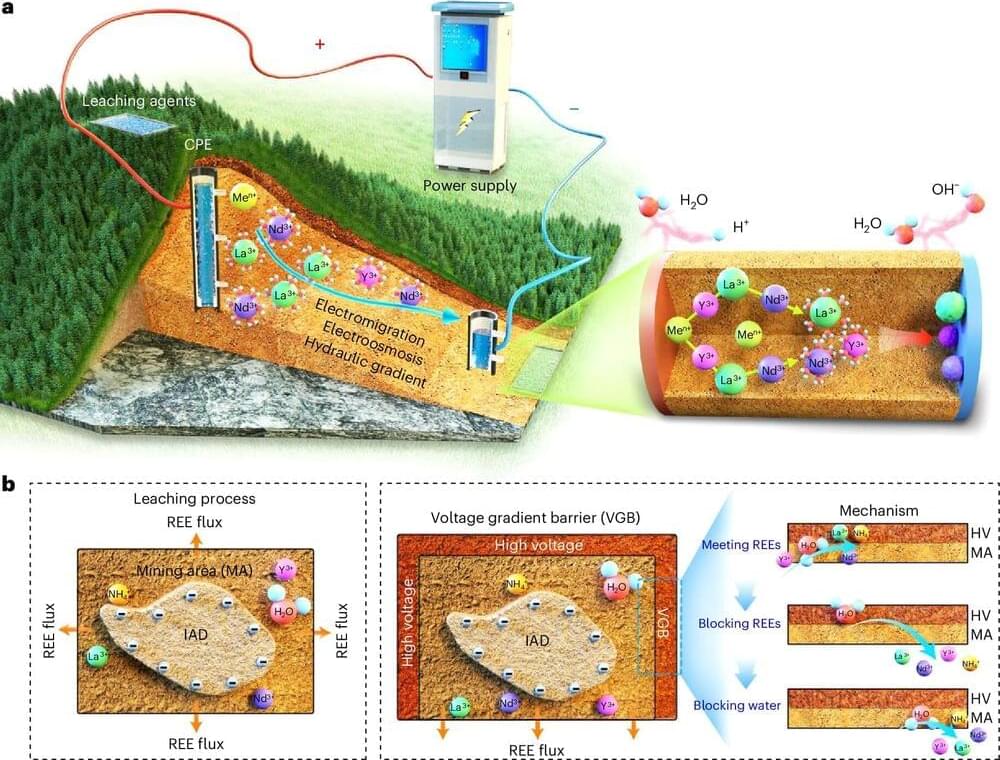
Toggle light / dark theme

Researchers led by Giulia Galli at University of Chicago’s Pritzker School of Molecular Engineering report a computational study that predicts the conditions to create specific spin defects in silicon carbide. Their findings, published online in Nature Communications, represent an important step towards identifying fabrication parameters for spin defects useful for quantum technologies.

Electronic spin defects in semiconductors and insulators are rich platforms for , sensing, and communication applications. Defects are impurities and/or misplaced atoms in a solid and the electrons associated with these carry a spin. This quantum mechanical property can be used to provide a controllable qubit, the basic unit of operation in quantum technologies.

Yet the synthesis of these spin defects, typically achieved experimentally by implantation and annealing processes, is not yet well understood, and importantly, cannot yet be fully optimized. In —an attractive host material for spin qubits due to its industrial availability—different experiments have so far yielded different recommendations and outcomes for creating the desired spin defects.

Researchers at the Indian Institute of Science (IISc) have developed a fully indigenous gallium nitride (GaN) power switch that can have potential applications in systems like power converters for electric vehicles and laptops, as well as in wireless communications. The entire process of building the switch—from material growth to device fabrication to packaging—was developed in-house at the Center for Nano Science and Engineering (CeNSE), IISc.

Due to their and efficiency, GaN transistors are poised to replace traditional silicon-based transistors as the in many , such as ultrafast chargers for , phones and laptops, as well as space and military applications such as radar.

“It is a very promising and disruptive technology,” says Digbijoy Nath, Associate Professor at CeNSE and corresponding author of the study published in Microelectronic Engineering. “But the material and devices are heavily import-restricted … We don’t have gallium nitride wafer production capability at commercial scale in India yet.” The know-how of manufacturing these devices is also a heavily-guarded secret with few studies published on the details of the processes involved, he adds.

Scientists unveil exciting possibilities for the development of highly efficient quantum devices.

Quantum mechanics is a branch of physics that explores the properties and interactions of particles at very small scale, such as atoms and molecules. This has led to the development of new technologies that are more powerful and efficient compared to their conventional counterparts, causing breakthroughs in areas such as computing, communication, and energy.

A quantum leap in engine design.

NVIDIA “Huang’s Law” is the primary catalyst for driving chip performance and efficiency to over 1000x in less than a decade. For NVIDIA, Huang’s Law is the fundamental approach that moves beyond traditional chip speedup fundamentals such as Moore’s Law which had dominated the tech industry in the past.

Huang’s Law To Dominate The Future For NVIDIA, Chip Shrinking In No Way Defines The Increment in Performance

NVIDIA’s CEO Jensen Huang has expressed multiple times that Moore’s Law is “slowing down,” and the concept it is backed with is starting to get outdated. The argument became heated, especially after Jensen’s GTC 2023 keynote. If we look at what Moore’s Law is, it is related to the number of transistors on a microchip and how it “should” double every year.

CERN’s data store has now crossed the remarkable capacity threshold of one exabyte, meaning that CERN has one million terabytes of disk space ready for data!

CERN’s data store not only serves LHC physics data, but also the whole spectrum of experiments and services needing online data management. This data capacity is provided using 111 000 devices, predominantly hard disks along with an increasing fraction of flash drives. Having such a large number of commodity devices means that component failures are common, so the store is built to be resilient, using different data replication methods. These disks, most of which are used to store physics data, are orchestrated by CERN’s open-source software solution, EOS, which was created to meet the LHC’s extreme computing requirements.

“We reached this new all-time record for CERN’s storage infrastructure after capacity extensions for the upcoming LHC heavy-ion run,” explains Andreas Peters, EOS project leader. “It is not just a celebration of data capacity, it is also a performance achievement, thanks to the reading rate of the combined data store crossing, for the first time, the one terabyte per second (1 TB/s) threshold.”

YouTube channel Moore’s Law Is Dead leaked two new allegedly official AMD slides detailing key specifications and IPC targets for Zen 5 and Zen 6. The new slides report that Zen 5 will be a significant architectural overhaul over Zen 4, targeting 10 to 15% IPC improvements or more. Zen 5 will also reportedly incorporate 16 core CCXs for the first time. Before we go much further, we’ll need to sprinkle a healthy amount of salt on this report.


A new leak has revealed highly in-depth architectural details about AMD’s Zen 5 and Zen 6 CPU architectures, including core architectural improvements and IPC gains.

I have to share this because it is a gem. My Kenyan business is gemstones 🙄 because Kenya is not far from Tanzanite. Anyways, here is free software for all you video creators. If you want to pay for it, it is $300 for the studio version. The same company also makes hardware for color correction, so you don’t drag a mouse you twist knobs.


Professional video editing, color correction, visual effects and audio post production all in a single application. Free and paid versions for Mac, Windows and Linux.