New light activated cancer treatment.
Several antibodies and antibody fragments have been previously developed for the treatment of various diseases, including cancer3,4. These antibodies bind to cell surface receptors expressed at higher levels on cancer cells, addressing a major challenge of selective cell targeting in cancer therapy. Although full-length antibodies have shown promise for treatment of several cancers, limited success has been demonstrated in eliminating solid tumors. Due to their large size, full-length antibodies are unable to diffuse deep into solid tumors5. In addition, it has been shown that high-affinity antibodies bind to the periphery of the tumor tissues, forming a barrier and preventing their further penetration6. Some studies in patients with cancer estimate that only 0.01% of the injected antibodies accumulate per gram of solid tumor tissue7. Small antibody fragments with low molecular weight can diffuse much deeper into tissues, presenting an excellent alternative to full-length antibodies. However, small antibody fragments have a low residence time in the body and often have a higher rate of dissociation (koff) from the target compared with full-length antibodies, limiting their clinical utility8. To address these challenges, antibody fragments are often multimerized9,10 and/or conjugated to larger proteins11, which increases the size of antibody fragments, again reducing their ability to penetrate into the tumor.
One solution to overcome the limitation of low residence time would be to replace the noncovalent interactions between the antibody fragment and its antigen with a covalent bond. In a notable effort, an affibody containing a photocrosslinker in its antigen binding region was shown to covalently link to its antigen and demonstrated higher accumulation on tumor tissues12. Another pioneering study involved developing affibodies containing a latent bioreactive amino acid in their antigen binding region that forms a covalent bond with the target antigen by proximity-dependent reaction without any external impetus13. However, the former had substantially lower binding affinity compared with its wild-type (wt) counterpart and thus, requires using a high concentration for efficient initial binding, while the latter could react with target antigen expressed on healthy cells causing side effects.
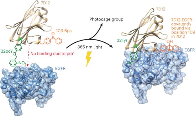
Although antibody-based therapeutics are more selective than several cytotoxic small molecule drugs used for cancer treatment, they can cause cardiac toxicity and skin reactions14. These side effects are due to the binding of the antibody to its receptor antigen expressed on healthy cells. This challenge could be addressed by activating antibody–antigen binding in the tumor microenvironment. One notable example in this direction is the development of antibodies containing an inhibitory N-terminal domain that is removed by tumor-specific proteases15. However, this approach would be difficult to extend to antibody fragments whose N terminus is not involved in antigen binding. We and others have also developed light-activated antibody fragments either by site-specific installation of photocaged functional groups or by introducing light-responsive proteins into antibodies16,17,18. In principle, such antibodies could be activated at the site of tumors using surgically implanted biocompatible light-emitting diodes (LEDs)19, thereby reducing the side effects of antibody-based therapeutics.


