БЛОГ

Archive for the ‘computing’ category: Page 368

Mar 24, 2022

New technique opens door to cheaper semiconductors, higher chip yield

Posted by in categories: computing, mobile phones, nanotechnology

Scientists from the NTU Singapore and the Korea Institute of Machinery & Materials (KIMM) have developed a technique to create a highly uniform and scalable semiconductor wafer, paving the way to higher chip yield and more cost-efficient semiconductors.

Left: Image of a six-inch silicon wafer with printed metal layers and its top-view scanning electron microscope image. Right: Image of the six-inch silicon wafer with nanowires and its cross-sectional scanning electron microscope image. (Image: NTU Singpore)

Semiconductor chips commonly found in smart phones and computers are difficult and complex to make, requiring highly advanced machines and special environments to manufacture.

Mar 24, 2022

A new class of materials for nanopatterning

Posted by in categories: computing, nanotechnology

The microscopic components that make up computer chips must be made at staggering scales. With billions of transistors in a single processor, each made of multiple materials carefully arranged in patterns as thin as a strand of DNA, their manufacturing tools must also operate at a molecular level.

Typically, these tools involve using stencils to selectively pattern or remove materials with high fidelity, layer after layer, to form nanoscale electronic devices. But as chips must fit more and more components to keep up with the digital world’s growing computational demands, these nanopatterning stencils must also become smaller and more precise.

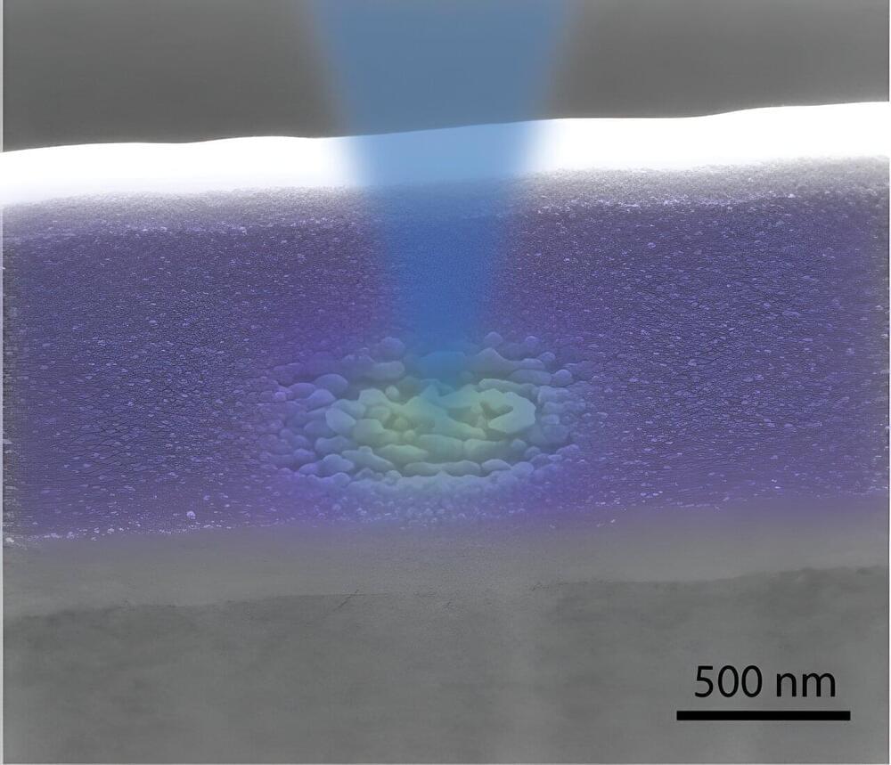
Now, a team of Penn Engineers has demonstrated how a new class of polymers could do just that. In a new study, the researchers demonstrated how “multiblock” copolymers can produce exceptionally ordered patterns in thin films, achieving spacings smaller than three nanometers.

Mar 24, 2022

How Can Quantum Computing Change the World?

Posted by in categories: business, climatology, computing, health, quantum physics

Every industry will be affected by quantum computing. They will alter the way business is done and the security systems in place which protect data, how we battle illnesses and create new materials, as well as how we tackle health and climate challenges.

As the race to build the first commercially functional quantum computer heats up, here we discuss a handful of the ways quantum computing will alter our world.

Mar 24, 2022

The future of PSUs is here: Intel’s ATX 3.0 powers monster 600W graphics cards

Posted by in categories: computing, futurism

PC power supplies haven’t seen a whole lot of change in the last decade or two. We’ve gotten modular cables for easier routing, smaller standards for itty-bitty builds, and that’s about it. But today Intel has finalized the ATX 3.0 standard, coming soon to a full-sized PC case near you. The biggest addition announced today is a new standardized connection for graphics cards and other PCIe devices, delivering up to 600 watts on a single connector.

Currently graphics cards are in a bit of a power pinch. The maximum throughput for an 8-pin ATX rail is 150 watts, so the biggest and most power-hungry GPUs need to double or even triple up, adding extra space requirements and more complex cable routing inside the case. The new 12-pin 12VHPWR connection should be able to deliver more energy than even the most powerful graphics cards need for the next generation or two. Each pin housing is also physically smaller, with a 3.0mm pitch versus 4.2mm on current power supply rails.

Technically it’s 16 total pins (12+4), with four additional data pins squeezed in beneath the primary power pins. This is to manage DC output voltage regulation and a series of new tools designed to regulate high power output efficiently and safely, all handled intelligently by the power supply. According to Intel, the new 12VHPWR connection will be the standard for “most, if not all” PCIe cards using the 5.0 spec.

Mar 23, 2022

Direct generation of complex structured light

Posted by in category: computing

Extension of laser beam structures promises new laser applications. Exploration of how beam structures change during nonlinear frequency conversion processes has drawn increasing interest in recent years. Nonlinear conversion is an excellent route for structured beam generation and represents a growing, hybrid field for researchers in nonlinear optics and laser technology, as well as the emerging area of light-field regulation technology.

For structured and nonlinear frequency conversion, researchers have considered both intracavity oscillation and external cavity spatial modulation. To achieve flexible outputs, spatial light modulators can be used to obtain structured beams both inside and outside the cavity. But this is an indirect, inefficient method. Intracavity nonlinear frequency generation of structured beams offers a direct, efficient method that has only rarely been investigated, until recently.

Inside a laser cavity, an effect known as “transverse mode locking” (TML) enables the direct generation of the vortex beams or optical vortices from a laser cavity. It is known that both solid-state microchip lasers and VCSELs can produce quite similar outputs of TML beam patterns under large Fresnel number pumping conditions. The complex transverse patterns formed by the TML effect, commonly composed of different basic modes with different weight coefficients and different locking phases, make for abundant spatial information in fundamental frequency modes. Nonlinear frequency conversion of these directly generated TML beams is of great interest, but not yet well studied.

Mar 22, 2022

Moore’s Law, 1970–2100

Posted by in category: computing

These two graphs illustrate the exponential growth in chip transistor counts, from 1970 until 2100.

Mar 22, 2022

Home Made Scanning Electron Microscope Shows Some Potential

Posted by in categories: computing, electronics

Scanning electron microscopes are one of those niche instruments that most of us don’t really need all the time, but would still love to have access to once in a while. Although we’ve covered a few attempts at home-builds before, many have faltered, except this project over on Hackday. IO by user Vini’s Lab, which appears to be still under active development. The principle of the SEM is pretty simple; a specially prepared sample is bombarded with a focussed beam of electrons, that is steered in a raster pattern. A signal is acquired, using one of a number of techniques, such as secondary electronics (SE) back-scattered electrons (BSE) or simply the transmitted current into the sample. This signal can then be used to form an image of the sample or gather other properties.

The project is clearly in the early stages, as the author says, it’s a very costly thing to build, but already some of the machined parts are ready for assembly. Work has started on the drive electronics for the condenser stigmata lens. This part of the instrument takes the central part of the rapidly diverging raw electron beam that makes it through the anode, and with a couple of sets of octopole coil sets, and an aperture or two, selects only the central portion of the beam, as well as correcting for any astigmatism in the beam. By adjusting the relative currents through each of the coils, a quadrupole magnetic field is created, which counteracts the beam asymmetry.

Scanning control and signal acquisition are handled by a single dedicated card, which utilises the PIO function of a Raspberry Pi Pico module. The Pico can drive the scanning operation, and with an external FTDI USB3.0 device, send four synchronised channels of acquired sample data back to the host computer. Using PCIe connectors and mating edge connectors on the cards, gives a robust and cost effective physical connection. As can be seen from the project page, a lot of mechanical design is complete, and machining has started, so this is a project to keep an eye on in the coming months, and possibly years!

Mar 22, 2022

Nvidia’s new Omniverse tools will make it easier than ever to build virtual worlds

Posted by in category: computing

“This is an answer to a huge demand we’ve had from a number of customers who wanted access to this platform but were limited because of the platform they’re on,” Richard Kerris, Nvidia’s Omniverse VP, said to reporters this week.

Omniverse Cloud is in early access now, and Nvidia is taking applications for it.

Next, Nvidia announced Omniverse OVX, a computing system designed specifically to meet the needs of massive simulations — or industrial digital twins.

Mar 21, 2022

Lensless Camera Captures Cellular-Level 3D Details

Posted by in categories: computing, information science

Rice University researchers have tested a tiny lensless microscope called Bio-FlatScope, capable of producing high levels of detail in living samples. The team imaged plants, hydra, and, to a limited extent, a human.

A previous iteration of the technology, FlatCam, was a lensless device that channeled light through a mask and directly onto a camera sensor, aimed primarily outward at the world at large. The raw images looked like static, but a custom algorithm translated the raw data into focused images.

The device described in current research looks inward to image micron-scale targets such as cells and blood vessels inside the body, and even through skin. The technology combines a sophisticated phase mask to generate patterns of light that fall directly onto the chip, the researchers said. The mask in the original FlatCam looked like a barcode and limited the amount of light that passes through to the sensor.

Mar 21, 2022

AMD Releases Milan-X CPUs With 3D V-Cache: EPYC 7003 Up to 64 Cores and 768 MB L3 Cache

Posted by in categories: computing, futurism

There’s been a lot of focus on how both Intel and AMD are planning for the future in packaging their dies to increase overall performance and mitigate higher manufacturing costs. For AMD, that next step has been V-cache, an additional L3 cache (SRAM) chiplet that’s designed to be 3D die stacked on top of an existing Zen 3 chiplet, tripling the total about of L3 cache available. Today, AMD’s V-cache technology is finally available to the wider market, as AMD is announcing that their EPYC 7003X “Milan-X” server CPUs have now reached general availability.

As first announced late last year, AMD is bringing its 3D V-Cache technology to the enterprise market through Milan-X, an advanced variant of its current-generation 3rd Gen Milan-based EPYC 7,003 processors. AMD is launching four new processors ranging from 16-cores to 64-cores, all of them with Zen 3 cores and 768 MB L3 cache via 3D stacked V-Cache.

AMD’s Milan-X processors are an upgraded version of its current 3rd generation Milan-based processors, EPYC 7003. Adding to its preexisting Milan-based EPYC 7,003 line-up, which we reviewed back in June last year, the most significant advancement from Milan-X is through its large 768 MB of L3 cache using AMD’s 3D V-Cache stacking technology. The AMD 3D V-Cache uses TSMC’s N7 process node – the same node Milan’s Zen 3 chiplets are built upon – and it measures at 36 mm², with a 64 MiB chip on top of the existing 32 MiB found on the Zen 3 chiplets.