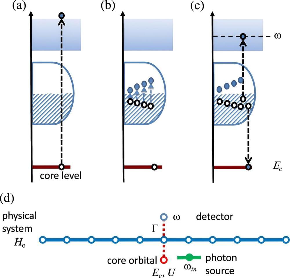
Toggle light / dark theme

IBM is building accessible, scalable quantum computing by focusing on three pillars:

**· **Increasing qubit counts.

**· **Developing advanced quantum software that can abstract away infrastructure complexity and orchestrate quantum programs.

**· **Growing an ecosystem of quantum-ready enterprises, organizations, and communities.

The next step in IBM’s goals to build a frictionless development experience will be the release of Qiskit Runtime in 2022, which will allow developers to build workflows in the cloud, offering greater flexibility. Bringing a serverless approach to quantum computing will also provide the flexibility to distribute workloads intelligently and efficiently across quantum and classical systems.

After a Sydney-based firm built the world’s first atomic-scale quantum integrated circuit.

Sydney-based firm Silicon Quantum Computing (SQC) built the first integrated silicon quantum computer circuit manufactured at the atomic scale, in what has been touted as a “major breakthrough” on the road to quantum supremacy, a press statement reveals.

The atomic-scale integrated circuit, which functions as an analog quantum processor, may be SQC’s biggest milestone since it announced in 2012 that it had built the world’s first single-atom transistor.

Researchers at the University of Central Florida are developing new photonic materials which may one day be used to enable ultra-fast, low-power light-based computing. The unique materials referred to as topological insulators, resemble wires that have been flipped inside out, with the insulation on the inside and the current flowing along the exterior.

In order to avoid the overheating issue that today’s ever-smaller circuits encounter, topological insulators could be incorporated into circuit designs to enable the packing of more processing power into a given area without generating heat.

The researchers’ most recent study, which was published on April 28 in the journal Nature Materials, presented a brand-new process for creating the materials that make use of a unique, chained honeycomb lattice structure. The linked, honeycombed pattern was laser etched onto a piece of silica, a material often used to create photonic circuits, by the researchers.

Australian scientists have created the world’s first-ever quantum computer circuit – one that contains all the essential components found on a classical computer chip but at the quantum scale.

The landmark discovery, published in Nature today, was nine years in the making.

“This is the most exciting discovery of my career,” senior author and quantum physicist Michelle Simmons, founder of Silicon Quantum Computing and director of the Center of Excellence for Quantum Computation and Communication Technology at UNSW told ScienceAlert.

Scientists at the Institute of Applied Physics at TU Dresden have come a step closer to the vision of a broad application of flexible, printable electronics. The team around Dr. Hans Kleemann has succeeded for the first time in developing powerful vertical organic transistors with two independent control electrodes. The results have recently been published in the renowned online journal Nature Communications.

High-definition roll-up televisions or foldable smartphones may soon no longer be unaffordable luxury goods that can be admired at international electronics trade fairs. High-performance organic transistors are a key necessity for the mechanically flexible electronic circuits required for these applications. However, conventional horizontal organic thin-film transistors are very slow due to the hopping-transport in organic semiconductors, so they cannot be used for applications requiring high frequencies. Especially for logic circuits with low power consumption, such as those used for Radio Frequency Identification (RFID), it is mandatory to develop transistors enabling high operation frequency as well as adjustable device characteristics (i.e., threshold-voltage). The research group Organic Devices and Systems (ODS) at the Dresden Integrated Center for Applied Photophysics (IAPP) of the Institute of Applied Physics headed by Dr.

Flashes of what may become a transformative new technology are coursing through a network of optic fibers under Chicago.

Researchers have created one of the world’s largest networks for sharing —a field of science that depends on paradoxes so strange that Albert Einstein didn’t believe them.

The network, which connects the University of Chicago with Argonne National Laboratory in Lemont, is a rudimentary version of what scientists hope someday to become the internet of the future. For now, it’s opened up to businesses and researchers to test fundamentals of quantum information sharing.

The library of two-dimensional (2D) layered materials keeps growing, from basic 2D materials to metal chalcogenides. Unlike their bulk counterparts, 2D layered materials possess novel features that offer great potential in next-generation electronics and optoelectronics devices.

Doping engineering is an important and effective way to control the peculiar properties of 2D materials for the application in logical circuits, sensors, and optoelectronic devices. However, additional chemicals have to be used during the process, which may contaminate the materials. The techniques are only possible at specific steps during material synthesis or device fabrication.

In a new paper published in eLight, a team of scientists led by Professor Han Zhang of Shenzhen University and Professor Paras N Prasad of the University of Buffalo studied the implementation of neutron-transmutation doping to manipulate . Their paper, titled has demonstrated the change for the first time.

For the first time, researchers have demonstrated an artificial organic neuron, a nerve cell, that can be integrated with a living plant and an artificial organic synapse. Both the neuron and the synapse are made from printed organic electrochemical transistors.

On connecting to the carnivorous Venus flytrap, the electrical pulses from the artificial nerve cell can cause the plant’s leaves to close, although no fly has entered the trap. Organic semiconductors can conduct both electrons and ions, thus helping mimic the ion-based mechanism of pulse (action potential) generation in plants. In this case, the small electric pulse of less than 0.6 V can induce action potentials in the plant, which in turn causes the leaves to close.

“We chose the Venus flytrap so we could clearly show how we can steer the biological system with the artificial organic system and get them to communicate in the same language,” says Simone Fabiano, associate professor and principal investigator in organic nanoelectronics at the Laboratory of Organic Electronics, Linköping University, Campus Norrköping.