Whether the light in our living spaces is on or off can be regulated in everyday life simply by reaching for the light switch. However, when the space for the light is shrunk to a few nanometers, quantum mechanical effects dominate, and it is unclear whether there is light in it or not. Both can even be the case at the same time, as scientists from the Julius-Maximilians-Universität Würzburg (JMU) and the University of Bielefeld show in the journal Nature Physics (“Identifying the quantum fingerprint of plasmon polaritons”).
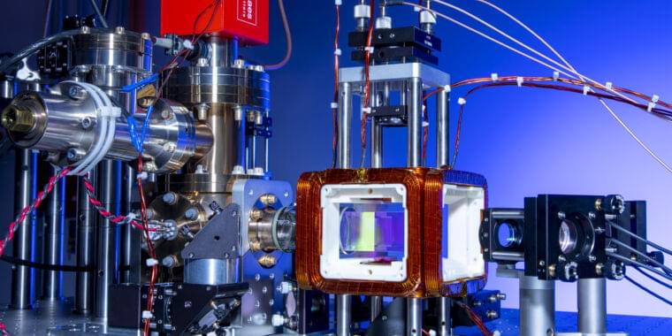
“Detecting these exotic states of quantum physics on the size scales of electrical transistors could help in the development of optical quantum technologies of future computer chips,” explains Würzburg professor Bert Hecht. The nanostructures studied were produced in his group.
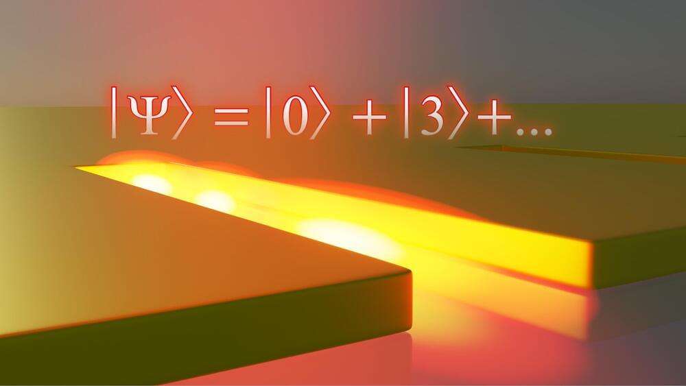
The technology of our digital world is based on the principle that either a current flows or it does not: one or zero, on or off. Two clear states exist. In quantum physics, on the other hand, it is possible to disregard this principle and create an arbitrary superposition of the supposed opposites. This increases the possibilities of transmitting and processing information many times over. Such superposition states have been known for some time, especially for the particles of light, so-called photons, and are used in the detection of gravitational waves.

