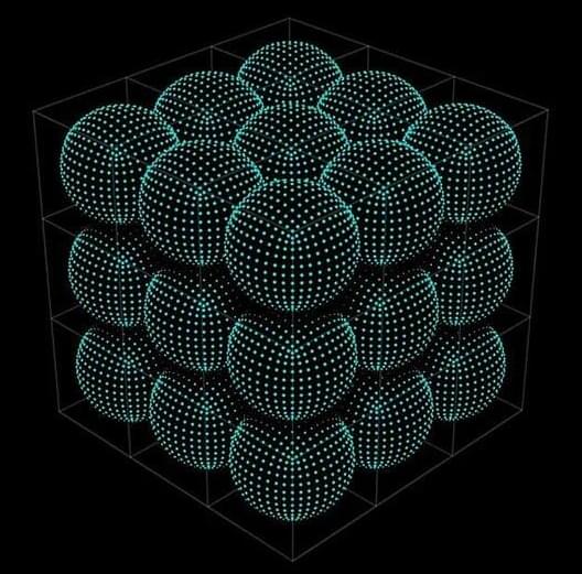
Space “cubically” with shapes that act like spheres? A proof at the intersection of geometry and theoretical computer science says yes.
A team of Stanford scientists claims to have tested a new brain-computer interface (BCI) that can decode speech at up to 62 words per minute, improving the previous record by 3.4 times.
That’d be a massive step towards real-time speech conversion at the pace of natural human conversation.
Max Hodak, who founded BCI company Neuralink alongside Elon Musk, but wasn’t involved in the study, called the research “a meaningful step change in the utility of implanted BCIs” in an email to Futurism.

So for those workers who have managed to hold on to their jobs, their working conditions are likely to get a little worse. For one, Github has announced that they’ll be switching to Microsoft Teams for their videoconferencing, and moving their laptop refresh schedule up to four years from the current three.
Could be worse, obviously, but still.
CEO Thomas Dohmke sent out an email to Github staff saying that “Although our entire leadership team has carefully deliberated this step and come to agreement, ultimately, as CEO the decision is mine. I recognize this will be difficult on you all, and we will approach this period with the utmost respect for every Hubber.”
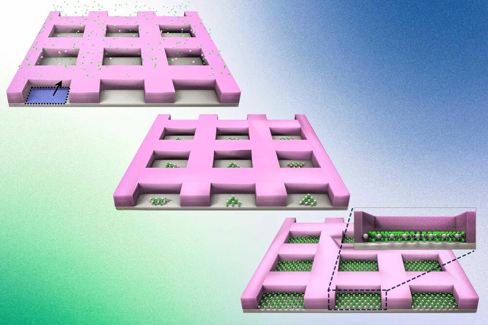
Adhering to Moore’s Law, the number of transistors on a microchip has doubled annually since the 1960s, but this growth is expected to reach its limit as silicon, the foundation of modern transistors, loses its electrical properties when devices made from it dip below a certain size.
Enter 2D materials — delicate, two-dimensional sheets of perfect crystals that are as thin as a single atom.
An atom is the smallest component of an element. It is made up of protons and neutrons within the nucleus, and electrons circling the nucleus.
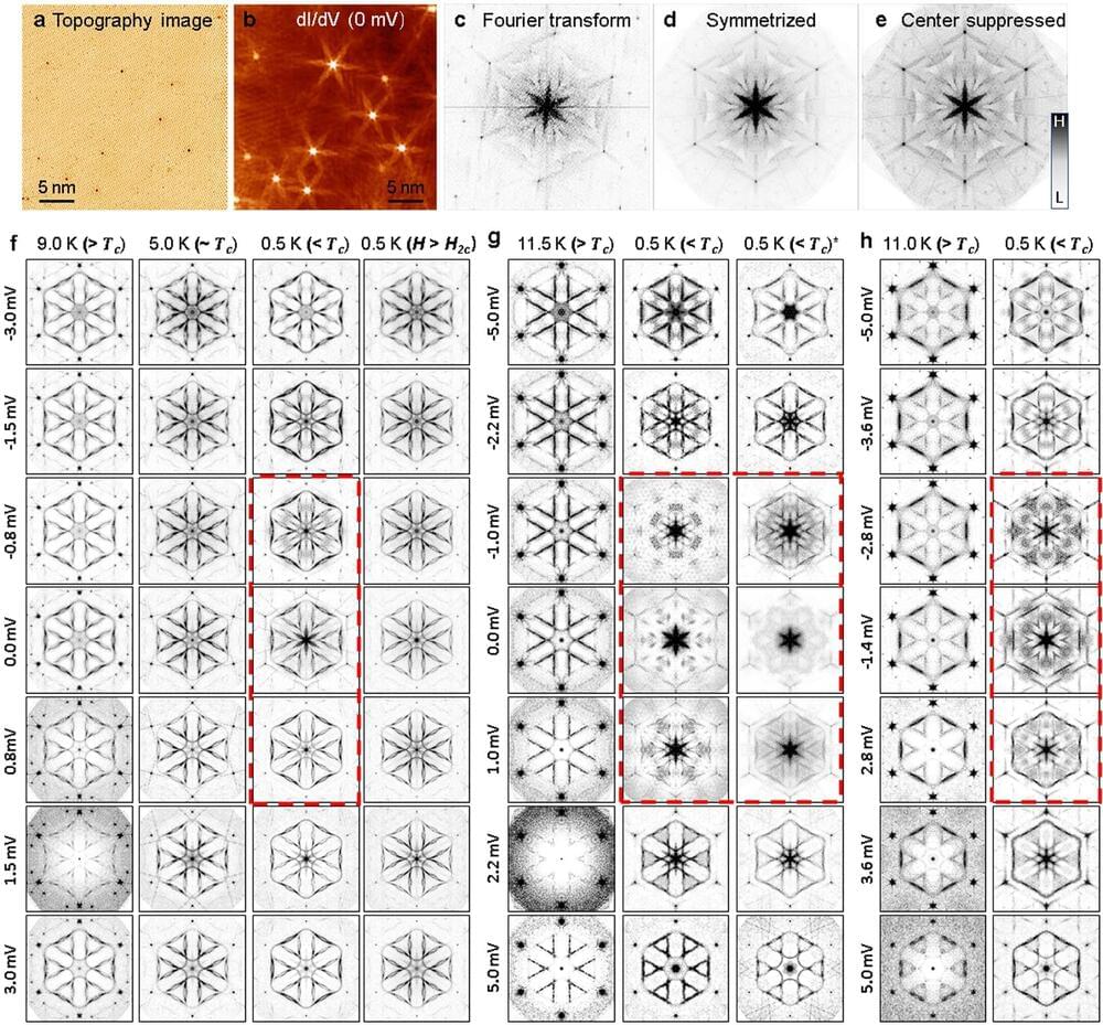
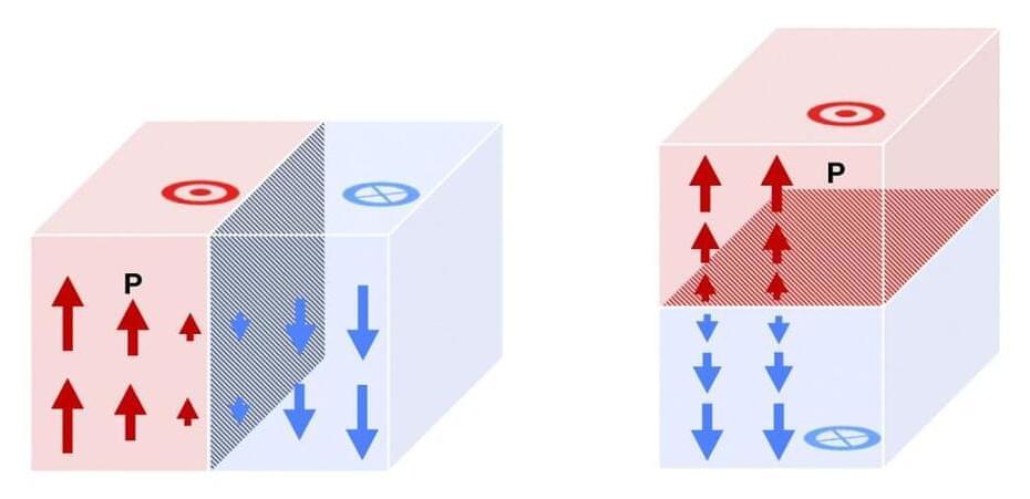
The University of Tennessee’s physicists have led a scientific team that found silicon—a mainstay of the soon-to-be trillion-dollar electronics industry—can host a novel form of superconductivity that could bring rapidly emerging quantum technologies closer to industrial scale production.
The findings are reported in Nature Physics and involve electron theft, time reversal, and a little electronic ambidexterity.
Superconductors conduct electric current without resistance or energy dissipation. Their uses range from powerful electromagnets for particle accelerators and medical MRI devices to ultrasensitive magnetic sensors to quantum computers. Superconductivity is a spectacular display of quantum mechanics in action on a macroscopic scale. It all comes down to the electrons.
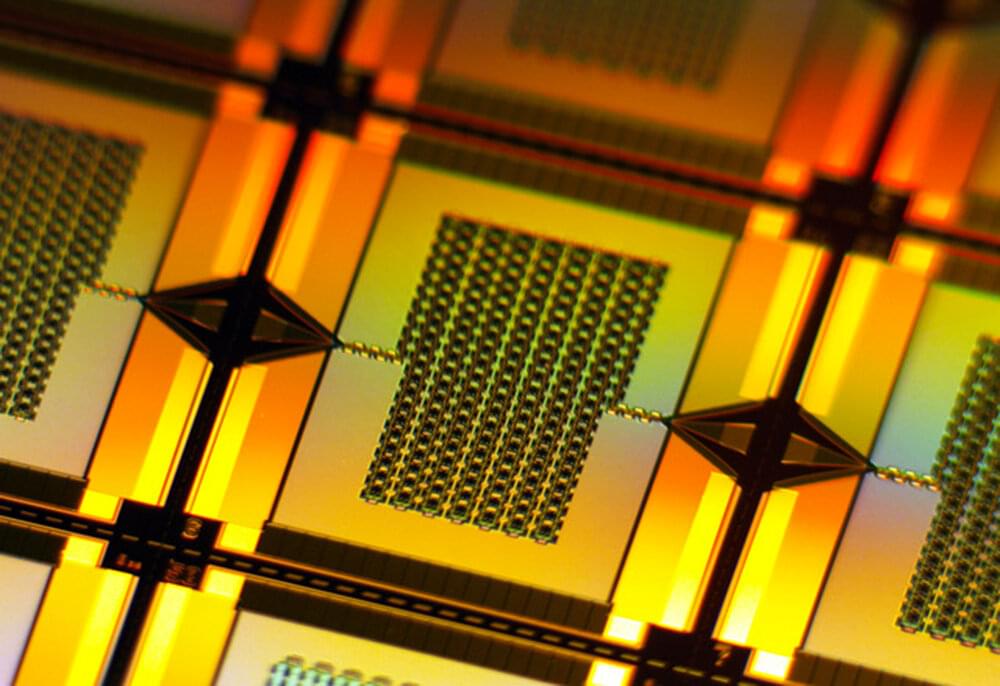
A certain amount of noise is inherent in any quantum system. For instance, when researchers want to read information from a quantum computer, which harnesses quantum mechanical phenomena to solve certain problems too complex for classical computers, the same quantum mechanics also imparts a minimum level of unavoidable error that limits the accuracy of the measurements.
Scientists can effectively get around this limitation by using “parametric” amplification to “squeeze” the noise—a quantum phenomenon that decreases the noise affecting one variable while increasing the noise that affects its conjugate partner. While the total amount of noise remains the same, it is effectively redistributed. Researchers can then make more accurate measurements by looking only at the lower-noise variable.
A team of researchers from MIT and elsewhere has now developed a new superconducting parametric amplifier that operates with the gain of previous narrowband squeezers while achieving quantum squeezing over much larger bandwidths. Their work is the first to demonstrate squeezing over a broad frequency bandwidth of up to 1.75 gigahertz while maintaining a high degree of squeezing (selective noise reduction). In comparison, previous microwave parametric amplifiers generally achieved bandwidths of only 100 megahertz or less.
For all of the unparalleled, parallel-processing, still-indistinguishable-from-magic wizardry packed into the three pounds of an adult human brain, it obeys the same rule as the other living tissue it controls: Oxygen is a must.
So it was with a touch of irony that Evgeny Tsymbal offered his explanation for a technological wonder—movable, data-covered walls mere atoms wide—that may eventually help computers behave more like a brain.
“There was unambiguous evidence that oxygen vacancies are responsible for this,” said Tsymbal, George Holmes University Professor of physics and astronomy at the University of Nebraska–Lincoln.
O.o! If the universe is some sorta hologram then this could be a clue to our actual reality.
Last December, the Nobel Prize in Physics was awarded for experimental evidence of a quantum phenomenon that has been known for more than 80 years: entanglement. As envisioned by Albert Einstein and his collaborators in 1935, quantum objects can be mysteriously correlated even when separated by great distances. But as strange as the phenomenon may seem, why is such an old idea still worthy of the most prestigious award in physics?
Coincidentally, just weeks before the new Nobel laureates were honored in Stockholm, another team of respected scientists from Harvard, MIT, Caltech, Fermilab and Google reported that they ran a process on Google’s quantum computer that could be interpreted as a wormhole. Wormholes are tunnels through the universe that can function as a shortcut through space and time and are loved by science fiction fans, and although the tunnel realized in this latest experiment only exists in a two-dimensional toy universe, it could be a breakthrough for the future represent research at the forefront of physics.
But why does entanglement have to do with space and time? And how can it be important for future breakthroughs in physics? Properly understood, entanglement means that the universe is what philosophers call “monistic,” that is, at the most fundamental level, everything in the universe is part of a single, unified whole. It is a defining property of quantum mechanics that its underlying reality is described in terms of waves, and a monistic universe would require universal functioning. Decades ago, researchers such as Hugh Everett and Dieter Zeh showed how our everyday reality can emerge from such a universal quantum mechanical description. But it is only now that researchers such as Leonard Susskind and Sean Carroll are developing ideas as to how this hidden quantum reality could explain not only matter but also the structure of space and time.
We gift Chukwuemeka Obi one of our pioneer students an iPhone 6 phone to enable him to browse and attend Zoom meetings. We need more of these phones and laptops to gift our students.
If there’s one thing I can’t stand it’s an uppity machine.
An excerpt from the 1968 film “2001: A Space Odyssey” directed by Stanley Kubrick.
Synopsis: Mankind finds a mysterious, obviously artificial, artifact buried on the moon and, with the intelligent computer HAL, sets off on a quest, where the way the HAL 9,000 super computer malfunctions.
© Metro-Goldwyn-Mayer Inc. (MGM)