Toggle light / dark theme

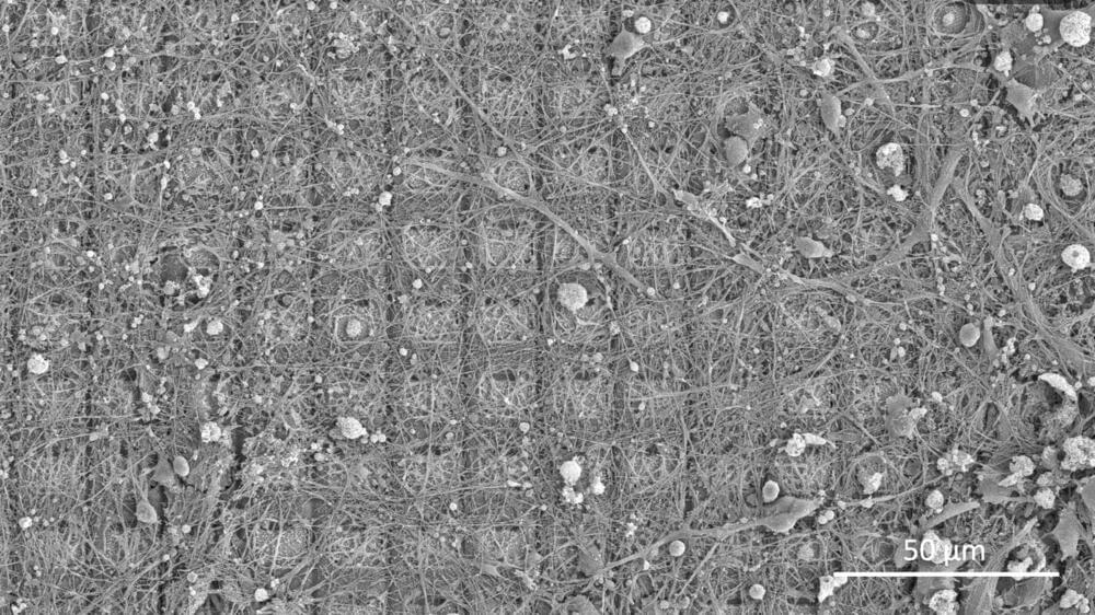
Researchers with the BrainGate Collaboration have deciphered the brain activity associated with handwriting: working with a 65-year-old (at the time of the study) participant with paralysis who has sensors implanted in his brain, they used an algorithm to identify letters as he attempted to write them; then, the system displayed the text on a screen; by attempting handwriting, the participant typed 90 characters per minute — more than double the previous record for typing with a brain-computer interface.

So far, a major focus of brain-computer interface research has been on restoring gross motor skills, such as reaching and grasping or point-and-click typing with a computer cursor.

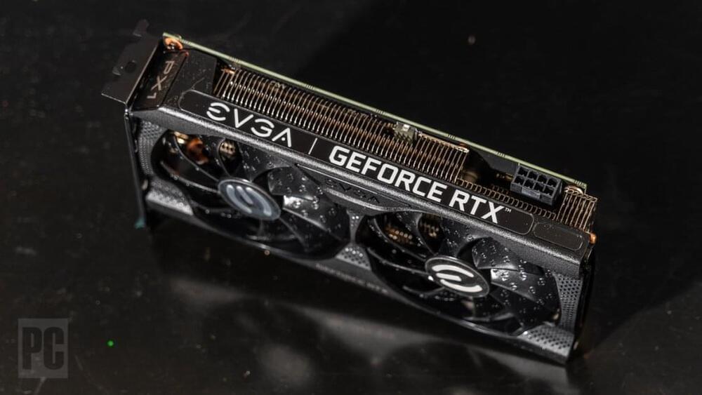
It’s bad out there for customers of electronic parts and components. The semiconductor shortage is so severe it’s being covered by mainstream media; meanwhile, various politicians have tasked their aides with looking at the global supply chain. Indeed, in the short term, the dearth of chips is already leading to product delays, companies redesigning their parts, and higher device prices. But over the long term, it could usher in a complete rethink of the way electronics parts are designed.

Peggy Carrieres, VP of global sales development and supplier enablement at Avnet, told me she expects the shortage to contribute to engineers reducing the number of physical components used and turning instead to software to handle functions that had historically been done in hardware. The shortages tied to the pandemic are an accelerator for this shift, but it has been happening for years as the industry adjusts to the end of Moore’s Law and the ability to eke out more performance at lower costs.

I had reached out to Avnet because I was interested in what it was seeing from its customers as the chip shortage dragged on. Avnet is a distributor, so it acts as a middleman between electronics components suppliers and the end customers of those parts. Someone building a new electronic device could work with Avnet to source the parts from an existing design, for example, or to build a design out of available parts that fit within a specific price.

A new way to form self-aligned ‘color centers’ promises scalability to over 10000 qubits for applications in quantum sensing and quantum computing.

Achieving the immense promise of quantum computing requires new developments at every level, including the computing hardware itself. A Lawrence Berkeley National Laboratory (Berkeley Lab)-led international team of researchers has discovered a way to use ion beams to create long strings of “color center” qubits in diamond. Their work is detailed in the journal Applied Physics Letters.

The authors includes several from Berkeley Lab: Arun Persaud, who led the study, and Thomas Schenkel, head of the Accelerator Technology and Applied Physics (ATAP) Division’s Fusion Science & Ion Beam Technology Program, as well as Casey Christian (now with Berkeley Lab’s Physics Division), Edward Barnard of Berkeley Lab’s Molecular Foundry, and ATAP affiliate Russell E. Lake.

Harnessing the Hum of Fluorescent Lights for More Efficient Computing

The property that makes fluorescent lights buzz could power a new generation of more efficient computing devices that store data with magnetic fields, rather than electricity.

A team led by University of Michigan researchers has developed a material that’s at least twice as “magnetostrictive” and far less costly than other materials in its class. In addition to computing, it could also lead to better magnetic sensors for medical and security devices.

Moore’s Law, the famous prediction that the number of transistors that can be packed onto a microchip will double every couple of years, has been bumping into basic physical limits. These limits could bring decades of progress to a halt, unless new approaches are found.

One new direction being explored is the use of atomically instead of silicon as the basis for new transistors, but connecting those “2D” materials to other conventional electronic components has proved difficult.

Now researchers at MIT, the University of California at Berkeley, the Taiwan Semiconductor Manufacturing Company, and elsewhere have found a new way of making those , which could help to unleash the potential of 2D materials and further the miniaturization of components—possibly enough to extend Moore’s Law, at least for the near future, the researchers say.

Scientists used to perform experiments by stirring biological and chemical agents into test tubes.

Nowadays, they automate research by using the size of postage stamps. In these tiny devices, millions of microscopic particles are captured in droplets of water, each droplet serving as the “test tube” for a single experiment. The chip funnels these many droplets, one at a time, through a tiny channel where a laser probes each passing droplet to record thousands of experimental results each second.

These chips are used for such things as testing new antibiotics, screening drug compounds, sequencing the DNA and RNA of single cells, and otherwise speeding up the pace of scientific discovery.