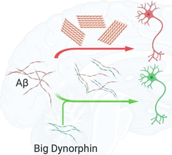
Toggle light / dark theme

The absence of piezoelectricity in silicon makes direct electromechanical applications of this mainstream semiconductor impossible. Integrated electrical control of the silicon mechanics, however, would open up new perspectives for on-chip actuorics. Here, we combine wafer-scale nanoporosity in single-crystalline silicon with polymerization of an artificial muscle material inside pore space to synthesize a composite that shows macroscopic electrostrain in aqueous electrolyte. The voltage-strain coupling is three orders of magnitude larger than the best-performing ceramics in terms of piezoelectric actuation. We trace this huge electroactuation to the concerted action of 100 billions of nanopores per square centimeter cross section and to potential-dependent pressures of up to 150 atmospheres at the single-pore scale. The exceptionally small operation voltages (0.4 to 0.9 volts), along with the sustainable and biocompatible base materials, make this hybrid promising for bioactuator applications.

An electrochemical change in the oxidation state of polypyrrole (PPy) can increase or decrease the number of delocalized charges in its polymer backbone (1). Immersed in an electrolyte, this is also accompanied by a reversible counter-ion uptake or expulsion and thus with a marcroscopic contraction or swelling under electrical potential control, making PPy one of the most used artificial muscle materials (15).

Here, we combine this actuator polymer with the three-dimensional (3D) scaffold structure of nanoporous silicon (68) to design, similarly as found in many multiscale biological composites in nature (9), a material with embedded electrochemical actuation that consists of a few light and abundant elemental constituents (i.e., H, C, N, O, Si, and Cl).

In the coming 2020s, the world of medical science will make some significant breakthroughs. Through brain implants, we will have the capability to restore lost memories.

~ The 2020s will provide us with the computer power to make the first complete human brain simulation. Exponential growth in computation and data will make it possible to form accurate models of every part of the human brain and its 100 billion neurons.

~ The prototype of the human heart was 3D printed in 2019. By the mid- 2020s, customized 3D- printing of major human body organs will become possible. In the coming decades, more and more of the 78 organs in the human body will become printable.

…As we enter into the next few decades, we will have the technologies that grant us the possibility of immortality, albeit one that is highly subjective.

With our ability to 3D print new body organs, our ability to use nanotechnology in fighting death at cellular levels, our ability to use CRISPR or other gene-editing technology to rewrite our definition of humans and even our ability to capture and extend our consciousness beyond the confines of the biological weakness of our human bodies — immortality may be within reach of our fingers as depicted in the painting of Michelangelo.

Synthetic biology startups raised some $3 billion through the first half of 2020, up from $1.9 billion for all of 2019, as the field brings the science of engineering to the art of life.

The big picture: Synthetic biologists are gradually learning how to program the code of life the way that computer experts have learned to program machines. If they can succeed — and if the public accepts their work — synthetic biology stands to fundamentally transform how we live.

What’s happening: SynBioBeta, synthetic biology’s major commercial conference, launched on Tuesday, virtually bringing together thousands of scientists, entrepreneurs, VCs and more to discuss the state of the field.

To operate safely and reliably in outdoor environments, electronic devices should be resistant to a wide variety of external factors, including radiation. In fact, high-energy radiation can damage several components of field-effect transistors (FETs) commonly used to make electronics, including their superconducting channel, gate oxide and the insulating materials surrounding it (e.g., isolation or substrate oxides).

For several years, research teams worldwide have thus been trying to devise strategies that could make more resistant to radiation. So far, however, this has proved to be highly challenging, and only a few of the techniques proposed in the past have achieved promising results.

Researchers at Peking University, the Chinese Academy of Sciences and Shanghai Tech University have recently fabricated a radiation-hardened and repairable integrated circuit (IC) based on carbon nanotube transistors with ion gel . This IC, first presented in a paper pre-published in Nature Electronics, could be used to build new that are more resistant to high-energy radiation.

A team of University of Arkansas physicists has successfully developed a circuit capable of capturing graphene’s thermal motion and converting it into an electrical current.

“An energy-harvesting circuit based on could be incorporated into a chip to provide clean, limitless, low-voltage power for small devices or sensors,” said Paul Thibado, professor of physics and lead researcher in the discovery.

The findings, published in the journal Physical Review E, are proof of a theory the physicists developed at the U of A three years ago that freestanding graphene—a single layer of carbon atoms—ripples and buckles in a way that holds promise for energy harvesting.

Researchers build circuit that harnessed the atomic motion of graphene to generate an electrical current that could lead to a chip to replace batteries.

A team of University of Arkansas physicists has successfully developed a circuit capable of capturing graphene’s thermal motion and converting it into an electrical current.

“An energy-harvesting circuit based on graphene could be incorporated into a chip to provide clean, limitless, low-voltage power for small devices or sensors,” said Paul Thibado, professor of physics and lead researcher in the discovery.

As our lives become increasingly intertwined with technology—whether supporting communication while working remotely or streaming our favorite show—so too does our reliance on the data these devices create. Data centers supporting these technology ecosystems produce a significant carbon footprint—and consume 200 terawatt hours of energy each year, greater than the annual energy consumption of Iran. To balance ecological concerns yet meet growing demand, advances in microelectronic processors—the backbone of many Internet of Things (IoT) devices and data hubs—must be efficient and environmentally friendly.

Northwestern University materials scientists have developed new design principles that could help spur development of future quantum materials used to advance (IoT) devices and other resource-intensive technologies while limiting ecological damage.

“New path-breaking materials and computing paradigms are required to make more energy-lean in the future,” said James Rondinelli, professor of materials science and engineering and the Morris E. Fine Professor in Materials and Manufacturing at the McCormick School of Engineering, who led the research.

That’s big news for the most mysterious phase of matter—and maybe physics as we know it.


For the first time, scientists have observed an interaction of a rare and baffling form of matter called time crystals. The crystals look at a glance like “regular” crystals, but they have a relationship to time that both intrigues and puzzles scientists because of its unpredictability. Now, experts say they could have applications in quantum computing.“regular” crystals, but they have a relationship to time that both intrigues and puzzles scientists because of its unpredictability. Now, experts say they could have applications in quantum computing.

🤯 You love time travel. So do we. Let’s nerd out over it together.