Small, safer vessels could be ‘silicon chip’ that ushers in new nuclear age.
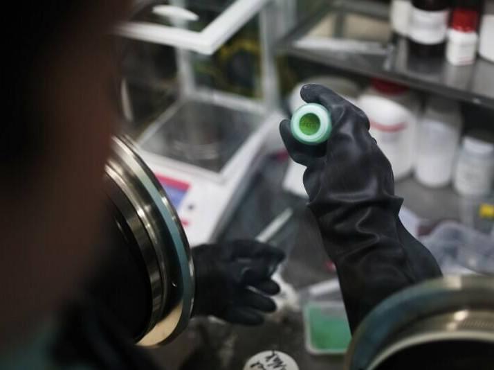


Quantum computing and communication often rely on the entanglement of several photons together. But obtaining these multiphoton states is a bit like playing the lottery, as generating entanglement between photons only succeeds a small fraction of the time. A new experiment shows how to improve one’s odds in this quantum game of chance. The method works like an entanglement assembly line, in which entangled pairs of photons are created in successive order and combined with stored photons.
The traditional method for obtaining multiphoton entanglement requires a large set of photon sources. Each source simultaneously generates an entangled photon pair, and those photons are subsequently interfered with each other. The process is probabilistic in that each step only succeeds in producing pair entanglement, say, once in every 20 tries. The odds become exponentially worse as entanglement of more and more photons is attempted.
Christine Silberhorn from Paderborn University, Germany, and her colleagues have developed a new method that offers a relatively high success rate [1]. They use a single source that generates pairs of polarization-entangled photons in succession. After the first pair is created, one of these photons is stored in an optical loop. When the source creates a new pair (which can take several tries), one of these photons is interfered with the stored photon. If successful, this interference creates a four-photon entangled state. The process can continue—with new pairs being generated and one photon being stored—until the desired multiphoton state is reached.
The rise of quantum computing and its implications for current encryption standards are well known. But why exactly should quantum computers be especially adept at breaking encryption? The answer is a nifty bit of mathematical juggling called Shor’s algorithm. The question that still leaves is: What is it that this algorithm does that causes quantum computers to be so much better at cracking encryption? In this video, YouTuber minutephysics explains it in his traditional whiteboard cartoon style.
“Quantum computation has the potential to make it super, super easy to access encrypted data — like having a lightsaber you can use to cut through any lock or barrier, no matter how strong,” minutephysics says. “Shor’s algorithm is that lightsaber.”
According to the video, Shor’s algorithm works off the understanding that for any pair of numbers, eventually multiplying one of them by itself will reach a factor of the other number plus or minus 1. Thus you take a guess at the first number and factor it out, adding and subtracting 1, until you arrive at the second number. That would unlock the encryption (specifically RSA here, but it works on some other types) because we would then have both factors.

Three scientists who laid the groundwork for the understanding of the odd “entangling” behavior of quantum particles have received the 2022 Nobel Prize in Physics.
French physicist Alain Aspect, Austria’s Anton Zeilinger and American John Clauser were honored for their experiments exploring the nature of entangled quantum particles.
Chipmaker Micron Technology revealed on Tuesday ambitious plans to develop a $100-billion computer chip factory complex in upstate New York, in a bid to boost domestic chip manufacturing and possibly deal with a worrying chips shortage. The money will be invested over a 20 year period, according to Reuters.
The world’s largest semiconductor fabrication facility
Micron claims the project will be the world’s largest semiconductor fabrication facility and will create nearly 50,000 jobs in New York alone. Currently, the largest semiconductor manufacturers in the world are: Intel Corp., Samsung, Taiwan Semiconductor Manufacturing Co. Ltd. (TSMC), SK Hynix, Micron Technology Inc., Qualcomm, Broadcom Inc., and Nvidia.
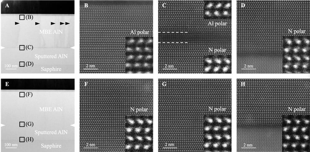
A group of researchers led by Cornell is unlocking the full potential of aluminum nitride—an important material for the advancement of electronics and photonics—thanks to the development of a surface cleaning technique that enables high-quality production.
The research was published Sept. 9 in the journal Science Advances. Graduate student Zexuan Zhang and research associate Yongjin Cho are the lead authors. The senior authors are Debdeep Jena and Huili Grace Xing, both professors of materials science and engineering and of electrical and computer engineering.
Aluminum nitride has gained significant research interest in the field of semiconductor materials as it provides an unmatched combination of high electrical resistivity and thermal conductivity, according to Zhang. The ceramic material is used as an electrically-insulating but thermally-conducting barrier in electronic devices, and due to its ability to operate at deep UV frequencies, it has great potential for use in light-emitting diodes and lasers.
Carnegie Mellon University researchers have pioneered the CMU Array—a new type of microelectrode array for brain computer interface platforms. It holds the potential to transform how doctors are able to treat neurological disorders.
The ultra-high-density microelectrode array (MEA), which is 3D-printed at the nanoscale, is fully customizable. This means that one day, patients suffering from epilepsy or limb function loss due to stroke could have personalized medical treatment optimized for their individual needs.
The collaboration combines the expertise of Rahul Panat, associate professor of mechanical engineering, and Eric Yttri, assistant professor of biological sciences. The team applied the newest microfabrication technique, Aerosol Jet 3D printing, to produce arrays that solved the major design barriers of other brain computer interface (BCI) arrays. The findings were published in Science Advances.

Electronic computing and communications have advanced significantly since the days of radio telegraphy and vacuum tubes. In fact, consumer devices now contain levels of processing power and memory that would be unimaginable just a few decades ago.
But as computing and information processing microdevices get ever smaller and more powerful, they are running into some fundamental limits imposed by the laws of quantum physics. Because of this, the future of the field may lie in photonics—the light-based parallel to electronics. Photonics is theoretically similar to electronics but substitutes photons for electrons. They have a huge potential advantage in that photonic devices may be capable of processing data much faster than their electronic counterparts, including for quantum computers.

Were you unable to attend Transform 2022? Check out all of the summit sessions in our on-demand library now! Watch here.
The open-source Linux operating system is an essential component of the cloud and enterprise application delivery. In fact, every cloud service, even Microsoft, offers Linux-based compute resources and Linux is often the default choice for embedded and internet of things (IoT) devices. Among the major Linux distribution vendors today are IBM’s Red Hat business unit, German vendor SUSE and Canonical, which develops the Ubuntu Linux distribution.
The market for Linux is forecast to grow to $22.15 billion by 2029, according to Fortune Business Insights, up from $6.27 billion in 2022.
