Toggle light / dark theme

Iontronic Circuits: Building Intelligence in Brine

Experiments with membranes offer a path toward scalable neuromorphic computing.

Imagine a future in which computers process information not with streams of electrons but with hydrated ions flowing through salt water, a system that mimics how the brain itself computes. This emerging field—known as iontronics, a portmanteau of ions and electronics—is rapidly growing as researchers design neuromorphic computing devices, inspired by animal nervous systems and powered by electrolyte solutions at the nanoscale [1–3]. Since Leon Chua introduced the memory resistor or “memristor” in the 1970s [4], these components have been considered revolutionary building blocks for neuromorphic computing. A memristor’s electrical resistance depends on the current that flowed through it before it was powered off, offering a way to store information. Unlike solid-state memristors, fluidic ones still face challenges in terms of scalability and integration with a circuit.

Electric signals reveal magnetic spin waves, hinting at faster computing

Today’s computers store information in magnetic hard drives, keeping files safe even when the device is powered off. But to run programs and process information, computers rely on electricity. Each calculation requires a transfer of information between the electric and magnetic systems. This back-and-forth is a major bottleneck in the speed of modern computing.

Devices that integrate magnetic components directly into computing logic would remove this limitation and allow computers to perform faster and more efficiently.

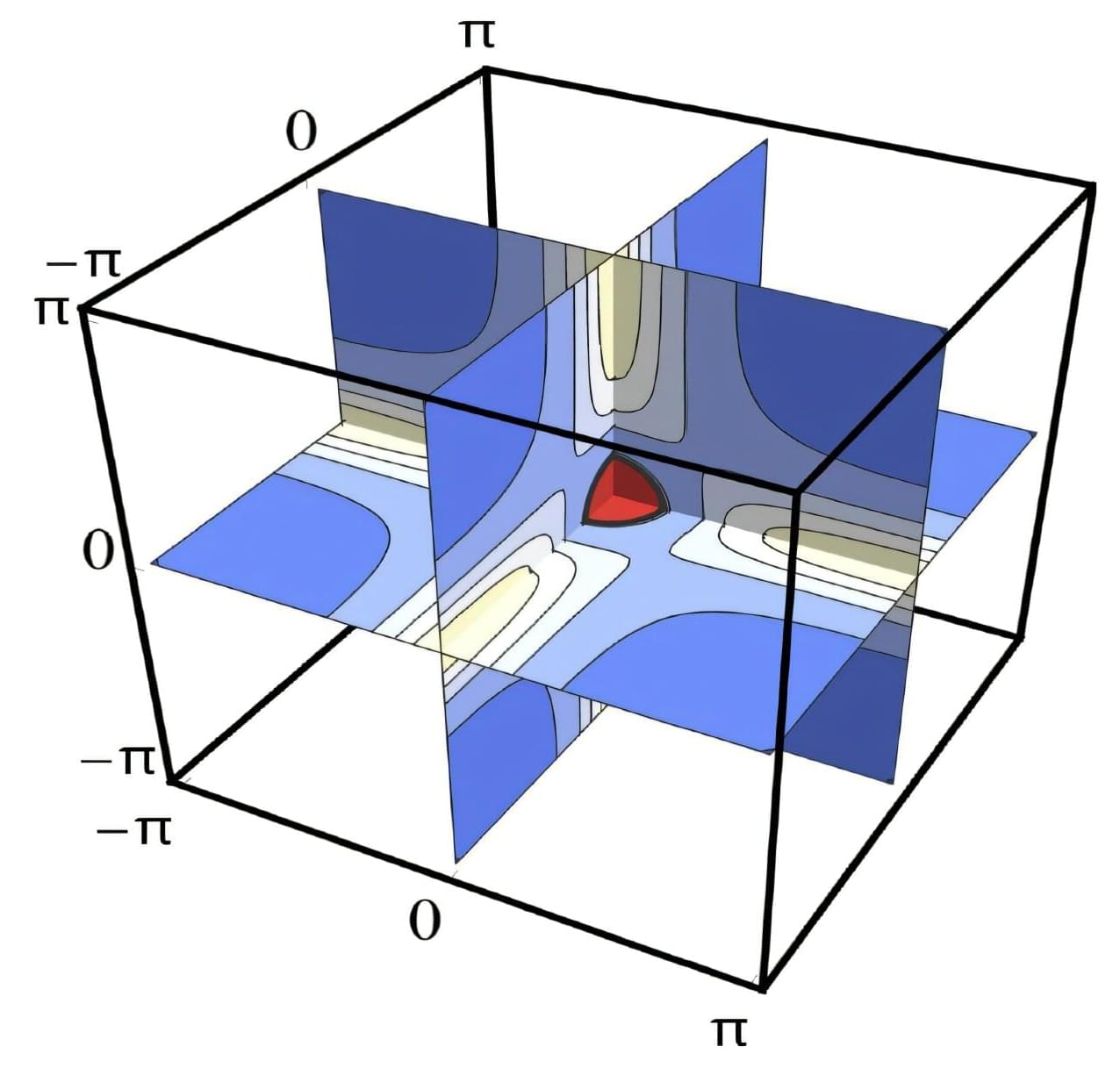
A new theoretical study led by University of Delaware engineers reveals that magnons, a type of magnetic spin wave, can produce detectable electric signals. The findings, published in the Proceedings of the National Academy of Sciences, highlight potential ways to control and manipulate magnons with electric fields and suggest a path toward integrating electric and magnetic components to enable next-generation computing technologies.

This Quantum Electron Breakthrough Could Make Computers Faster Than Ever Before

Auburn University scientists have developed a new class of materials that allow precise control over free electrons, potentially transforming computing and chemical manufacturing. Imagine a future where factories produce new materials and chemical compounds more quickly, more efficiently, and at

Scientists smash record in stacking semiconductor transistors for large-area electronics

King Abdullah University of Science and Technology (KAUST; Saudi Arabia) researchers have set a record in microchip design, achieving the first six-stack hybrid CMOS (complementary metal-oxide semiconductor) for large-area electronics. With no other reported hybrid CMOS exceeding two stacks, the feat marks a new benchmark in integration density and efficiency, opening possibilities in electronic miniaturization and performance.

A paper detailing the team’s research appears in Nature Electronics.

Among microchip technologies, CMOS microchips are found in nearly all electronics, from phones and televisions to satellites and medical devices. Compared with conventional silicon chips, hybrid CMOS microchips hold greater promise for large-area electronics. Electronic miniaturization is crucial for flexible electronics, smart health, and the Internet of Things, but current design approaches are reaching their limits.

Living computers powered by mushrooms

Mushrooms are known for their toughness and unusual biological properties, qualities that make them attractive for bioelectronics. This emerging field blends biology and technology to design innovative, sustainable materials for future computing systems.

Turning Mushrooms Into Living Memory Devices

Researchers at The Ohio State University recently discovered that edible fungi, such as shiitake mushrooms, can be cultivated and guided to function as organic memristors. These components act like memory cells that retain information about previous electrical states.

Mesoscale volumetric fluorescence imaging at nanoscale resolution by photochemical sectioning

I first explored this amazing work back when it was a preprint! Wang et al. herein developed VIPS (volumetric imaging via photochemical sectioning), a way of using UV light to remove layers of expanded tissue-hydrogel, allowing combination of high-resolution lattice-light sheet microscopy with expansion microscopy. Link: [ https://www.science.org/doi/10.1126/science.adr9109]

In my opinion, this technology has enormous future promise for high-throughput connectomics! They will need to improve their labeling density so that higher expansion factors can be used, but this problem is well-studied and I think the issue will likely be solvable with additional resources/effort.


Optical nanoscopy of intact biological specimens has been transformed by recent advancements in hydrogel-based tissue clearing and expansion, enabling the imaging of cellular and subcellular structures with molecular contrast. However, existing high-resolution fluorescence microscopes are physically limited by objective-to-specimen distance, which prevents the study of whole-mount specimens without physical sectioning. To address this challenge, we developed a photochemical strategy for spatially precise sectioning of specimens. By combining serial photochemical sectioning with lattice light-sheet imaging and petabyte-scale computation, we imaged and reconstructed axons and myelin sheaths across entire mouse olfactory bulbs at nanoscale resolution.

Pressure turns Ångström-thin semiconducting bismuth into a metal, expanding options for reconfigurable electronics

Two-dimensional (2D) materials, sparked by the isolation of Nobel-prize-winning graphene in 2004, has revolutionized modern materials science by showing that electrical, optical, and mechanical behaviors can be tuned simply by adjusting the thickness, strain, or stacking order of such 2D materials. From transistors and flexible display to neuromorphic chips, the future of electronics is expected to be significantly empowered by 2D materials.

In a new study published in Nano Letters titled “Pressure-Driven Metallicity in Ångström-Thickness 2D Bismuth and Layer-Selective Ohmic Contact to MoS2,” researchers led by SUTD have discovered that a gentle squeeze is enough to make bismuth—one of the heaviest elements in the periodic table—switch its electrical personality.

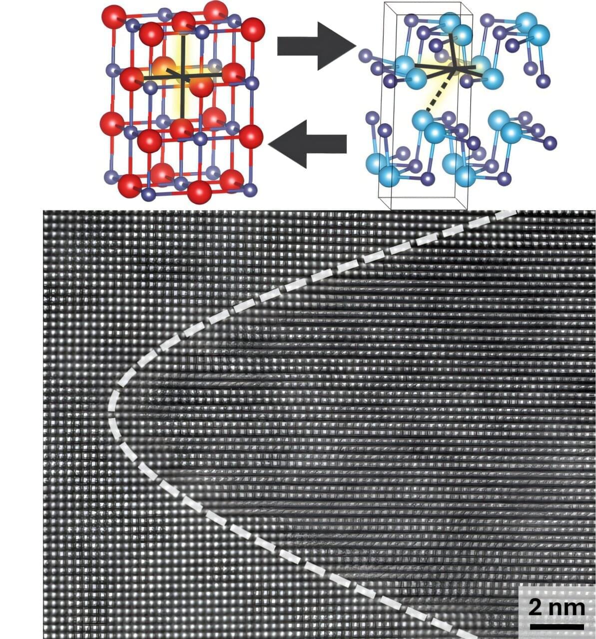
Using state-of-the-art density functional theory (DFT) simulations, the team showed that when a single layer of bismuth, only a few atoms thick, is compressed or “squeezed” between surrounding materials, the atoms reorganize from a slightly corrugated (or buckled) structure into a perfectly flat one. This structural flattening, though subtle, has dramatic electronic consequences: it eliminates the energy band gap and allows electrons to move freely, turning the material metallic.

Amazon: This week’s AWS outage caused by major DNS failure

Amazon says a major DNS failure was behind a massive AWS (Amazon Web Services) outage that took down many websites and online services on Monday.

As BleepinComputer reported earlier this week, this incident impacted a critical Northern Virginia data center in the US-EAST-1 region, affecting users worldwide, including the United States and Europe, for over 14 hours.

According to a post-mortem published on Thursday, a race condition caused a major DNS failure in Amazon DynamoDB’s infrastructure, specifically within its DNS management system that controls how user requests are routed to healthy servers, which led to the accidental deletion of all IP addresses for the database service’s regional endpoint.

/* */