To improve the ability of metapipeline-DNA to determine where changes in the genome have occurred, the scientists worked with the Genome in a Bottle Consortium led by the U.S. Department of Commerce’s National Institute of Standards and Technology. By incorporating this public-private-academic consortium’s meticulously validated resources, the researchers reduced the rate of false positives without reducing the tool’s precision in finding true genetic variants.
The researchers also produced two case studies demonstrating the pipeline’s capabilities for cancer research. The investigators used metapipeline-DNA to analyze sequencing data from five patients that donated both normal tissue and tumor samples, as well as another five from The Cancer Genome Atlas.
The next step is to get metapipeline-DNA into more labs to accelerate discoveries, and to continue improving the resource with more user feedback. ScienceMission sciencenewshighlights.
In a single experiment, scientists can decipher the entire genomes of many patient samples, animal models or cultured cells. To fully realize the potential to study biology at this unprecedented scale, researchers must be equipped to analyze the titanic troves of data generated by these new methods.
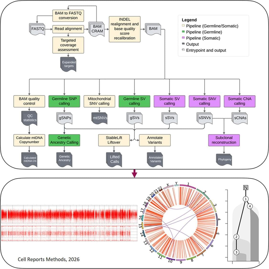
Scientists published findings in Cell Reports Methods discussing building and testing a new computational tool for tackling massive and complex sequencing datasets. The new resource, named metapipeline-DNA, may also make sequencing data analysis more standardized across different research labs.
The sequence of a single human genome represents about 100 gigabytes of raw data, the rough equivalent of 20,000 smartphone photos. The sheer scale of experimental data increases significantly as tens or hundreds of genomes are added into the mix.