NASA’s internship programs provide training, mentoring, and career development opportunities while working with the best science, engineering, financial, information technology and business minds in the world.
Category: engineering – Page 45
The Bernal Sphere Space Habitat
Discover the incredible engineering and visionary potential of Bernal Spheres, futuristic space habitats designed to sustain human life in the stars.
Watch my exclusive video Big Alien Theory https://nebula.tv/videos/isaacarthur–…
Get Nebula using my link for 40% off an annual subscription: https://go.nebula.tv/isaacarthur.
Get a Lifetime Membership to Nebula for only $300: https://go.nebula.tv/lifetime?ref=isa…
Use the link gift.nebula.tv/isaacarthur to give a year of Nebula to a friend for just $30.
Visit our Website: http://www.isaacarthur.net.
Join Nebula: https://go.nebula.tv/isaacarthur.
Support us on Patreon: / isaacarthur.
Support us on Subscribestar: https://www.subscribestar.com/isaac-a…
Facebook Group: / 1583992725237264
Reddit: / isaacarthur.
Twitter: / isaac_a_arthur on Twitter and RT our future content.
SFIA Discord Server: / discord.
Credits:
Megastructures: The Bernal Sphere.
Episode 485; February 6, 2025
Written, Produced & Narrated by: Isaac Arthur.
Editors: Ludwig Luska.
Graphics: Bryan Versteeg, Fishy Tree, Jeremy Jozwik, Udo Schroeter.
Select imagery/video supplied by Getty Images.
Music Courtesy of Epidemic Sound http://epidemicsound.com/creator.
Phase Shift, \
A new hydrogel semiconductor represents a breakthrough for tissue-interfaced bioelectronics
The ideal material for interfacing electronics with living tissue is soft, stretchable, and just as water-loving as the tissue itself—in short, a hydrogel. Semiconductors, the key materials for bioelectronics such as pacemakers, biosensors, and drug delivery devices, on the other hand, are rigid, brittle, and water-hating, impossible to dissolve in the way hydrogels have traditionally been built.
A paper published today in Science from the UChicago Pritzker School of Molecular Engineering (PME) has solved this challenge that has long stymied researchers, reimagining the process of creating hydrogels to build a powerful semiconductor in hydrogel form. Led by Asst. Prof. Sihong Wang’s research group, the result is a bluish gel that flutters like a sea jelly in water but retains the immense semiconductive ability needed to transmit information between living tissue and machine.
New material from the UChicago Pritzker School of Molecular Engineering can create better brain-machine interfaces, biosensors, and pacemakers.
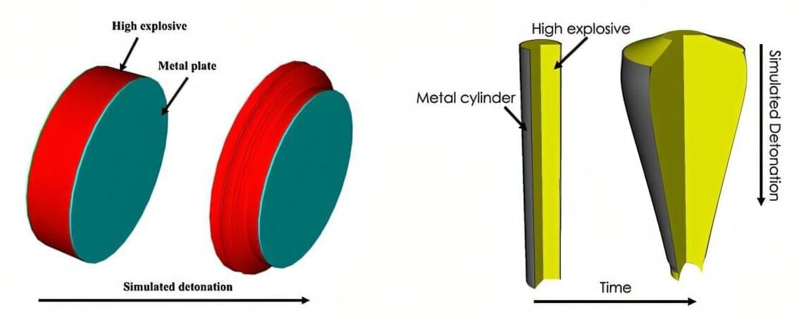
Quantifying metal strength uncertainty in high-explosives models
For the first time, a team of researchers at Lawrence Livermore National Laboratory (LLNL) quantified and rigorously studied the effect of metal strength on accurately modeling coupled metal/high explosive (HE) experiments, shedding light on an elusive variable in an important model for national security and defense applications.
The team used a Bayesian approach to quantify metal strength uncertainty with tantalum and two common explosive materials and integrated it into a coupled metal/HE model. Their findings could lead to more accurate models for equation-of-state-studies, which assess the state of matter a material exists in under different conditions. Their paper —featured as an editor’s pick in the Journal of Applied Physics —also suggested that metal strength uncertainty may have an insignificant effect on result.
“There has been a long-standing field lore that HE model calibrations are sensitive to the metal strength,” said Matt Nelms, the paper’s first author and a group leader in LLNL’s Computational Engineering Division (CED). “By using a rigorous Bayesian approach, we found that this is not the case, at least when using tantalum.”
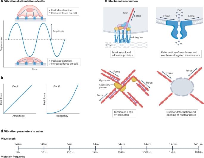
Vibration-based cell engineering
Vibration can be applied to cells in vitro and in vivo to trigger specific mechanotransductive pathways and guide cell-fate decisions. This Review explores the use of vibrational stimulation for cell engineering, outlining key pathways, devices and applications for this new mechanical cell-stimulation tool.
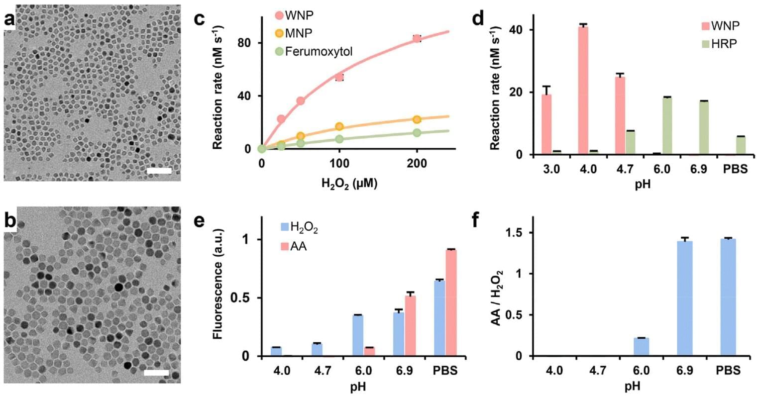
Magnetic nanoparticles with enzymatic activity could improve cancer therapy
Researchers at the University of Kentucky are exploring new ways to use nanoparticles in combination with other materials as an innovative approach to cancer therapy.
The paper titled “Iron Oxide Nanozymes Enhanced by Ascorbic Acid for Macrophage-Based Cancer Therapy” was published earlier this year in Nanoscale.
Sheng Tong, Ph.D., an associate professor in the F. Joseph Halcomb II, M.D., Department of Biomedical Engineering in the UK Stanley and Karen Pigman College of Engineering, led the study.

Harnessing chaos: How the brain turns randomness into robust memory
Random noise, such as background hubbub on a phone call, is usually thought of as unwanted interference. Now researchers at Columbia Engineering find the brain may harness unavoidable random fluctuations of its activity to perform useful computations, particularly in tasks relying on memory.
These findings not only deepen our understanding of how the brain works, but also may provide a blueprint for building smarter, more resilient technologies, the research team says.
They detailed their findings Jan. 16 in the Proceedings of the National Academy of Sciences.

Duke professor-led biotech company raises $175 million to advance epigenome editing therapy clinical trials
Tune Therapeutics, a Durham biotechnology startup co-founded by a Duke professor, announced the completion of its Series B fundraising round on Jan. 12, in which it raised $175 million to support clinical trials for its epigenome editor.
The company will use the funding to advance clinical trials for Tune-401, the epigenetic silencing drug for treating chronic Hepatitis B — a viral infection that damages the liver and affects millions globally. The investment will also support the development of various other therapies, including additional gene, cell and regenerative therapy programs.
“The goal is to epigenetically repress the virus to prevent it from being able to replicate and make the viral proteins that it would normally produce,” said Charles Gersbach, John W. Strohbehn distinguished professor of biomedical engineering and cofounder of Tune Therapeutics.
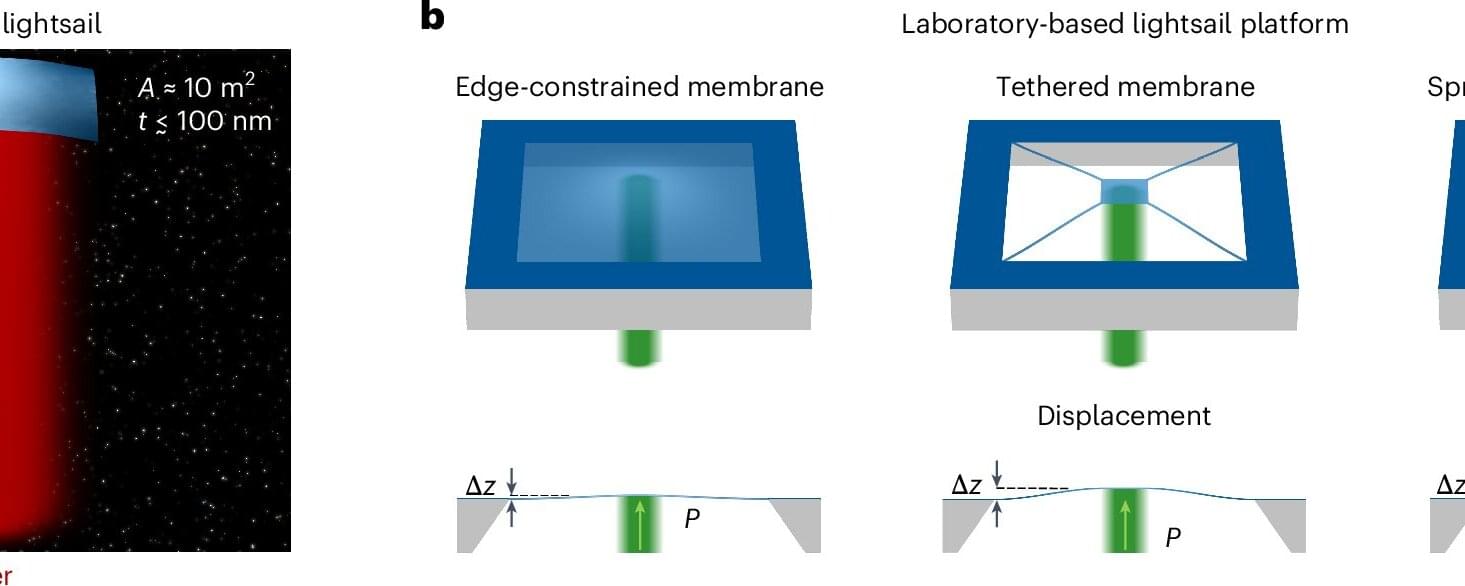
First steps taken toward developing interstellar lightsails
The idea of traveling through interstellar space using spacecraft propelled by ultrathin sails may sound like the stuff of sci-fi novels. But in fact, a program started in 2016 by Stephen Hawking and Yuri Milner, known as the Breakthrough Starshot Initiative, has been exploring the idea. The concept is to use lasers to propel miniature space probes attached to “lightsails” to reach ultrafast speeds and eventually our nearest star system, Alpha Centauri.
Caltech is leading the worldwide community working toward achieving this audacious goal.
“The lightsail will travel faster than any previous spacecraft, with potential to eventually open interstellar distances to direct spacecraft exploration that are now only accessible by remote observation,” explains Harry Atwater, the Otis Booth Leadership Chair of the Division of Engineering and Applied Science and the Howard Hughes Professor of Applied Physics and Materials Science at Caltech.
Accidental discovery of identical oil lenses offers insights into emulsions on fluid surfaces
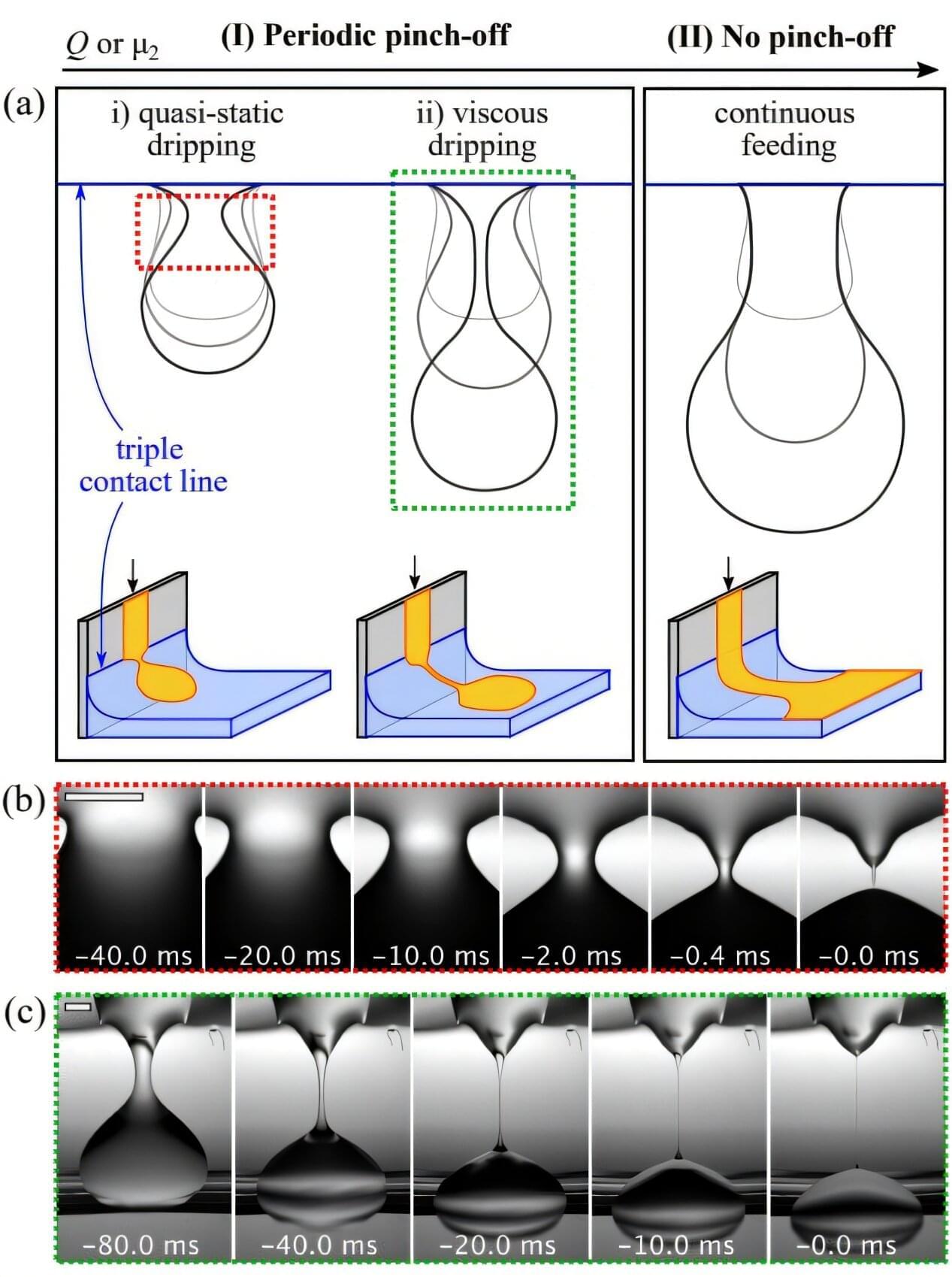
A team of researchers from Universidad Carlos III de Madrid (UC3M) has developed an innovative technique that allows the production of regular oil lenses of uniform size on the surface of water in a simple and reproducible fashion. The technique will facilitate the study of the behavior of oily substances dispersed on water surfaces.
This discovery is crucial for understanding the dispersion of some liquids floating on water and could have many applications in oil spill mitigation and the food and textile industries. The study is published in the journal Physical Review Letters.
The initial discovery, according to the researchers, was the result of an “accident” during the preparation of a routine experiment. “We were trying to coat a water surface with a thin layer of oil, but the result was unexpected: Instead of a uniform film, we obtained a series of identical and very small droplets, which aroused our curiosity,” explains Javier Rodríguez, from UC3M’s Department of Thermal and Fluids Engineering.