Scientists at Penn Engineering have developed a quantum sensing method that detects signals from individual atoms.

An international research team, working with cutting-edge technology at the University of Nebraska–Lincoln, has made a discovery that may dramatically expand the materials used in next-generation, energy-efficient memory and logic devices.
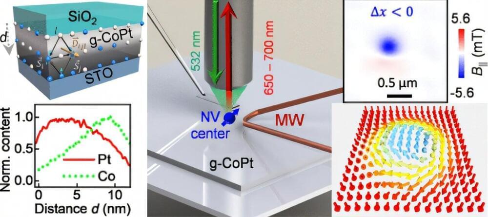
The team, which includes Nebraska’s Abdelghani Laraoui, assistant professor of mechanical and materials engineering, successfully demonstrated for the first time the imaging of magnetic skyrmions at room temperature in composition engineered magnetic materials. The team observed the tiny, vortex-like particles in these magnetic materials using a nitrogen-vacancy scanning probe in Laraoui’s lab. The findings are published in ACS Nano.
“This discovery is a huge step forward because, until now, scientists could only observe these skyrmions in bulk chiral magnetic materials at very low temperatures,” Laraoui said. “Being able to study them at room temperature opens up a whole new world of applications and possibilities.”

While most of us are familiar with magnets from childhood games of marveling at the power of their repulsion or attraction, fewer realize the magnetic fields that surround us—and the ones inside us. Magnetic fields are not just external curiosities; they play essential roles in our bodies and beyond, influencing biological processes and technological systems alike. A recent arXiv publication from the University of Chicago’s Pritzker School of Molecular Engineering and Argonne National Laboratory highlights how magnetic fields in the body may be analyzed using quantum-enabled fluorescent proteins, with hopes of applying to cell formation or early disease detection.
Detecting subtle changes in magnetic fields may equate to beyond subtle impacts in certain fields. For instance, quantum sensors could be applied to the detection of electromagnetic anomalies in data centers, potentially revealing evidence of malicious tampering. Similarly, they might be used to study changes in the brain’s electromagnetic signals, offering insights into neurological diseases such as the onset of dementia. However, these applications demand sensors that are not only sensitive but also capable of operating reliably in real-world conditions.
Spin qubits, known for their notable sensitivity to magnetic fields, are introduced in the study as a compelling solution. Traditionally, spin qubits have been formed from nitrogen-vacancy centers in diamonds. While these systems have demonstrated remarkable precision, the diamonds’ bulky size in relation to molecules and complex surface chemistry limit their usability in biological environments. This creates a need for a more adaptable and biologically compatible sensor.

Case Western Reserve University researcher advances zinc-sulfur battery technology. Rechargeable lithium-ion batteries power everything from electric vehicles to wearable devices. But new research from Case Western Reserve University suggests that a more sustainable and cost-effective alternative may lie in zinc-based batteries.
In a study published recently in Angewandte Chemie, researchers announced a significant step toward creating high-performance, low-cost zinc-sulfur batteries.
“This research marks a major step forward in the development of safer and more sustainable energy storage solutions,” said Chase Cao, a principal investigator and assistant professor of mechanical and aerospace engineering at Case School of Engineering. “Aqueous zinc-sulfur batteries offer the potential to power a wide range of applications — from renewable energy systems to portable electronics — with reduced environmental impact and reliance on scarce materials.”

A groundbreaking study showcases the creation of sustainable hydrophobic paper, enhanced by cellulose nanofibres and peptides, presenting a biodegradable alternative to petroleum-based materials, with potential uses in packaging and biomedical devices.
Researchers aimed to develop hydrophobic paper by leveraging the strength and water resistance of cellulose nanofibers, creating a sustainable, high-performance material suitable for packaging and biomedical applications. This innovative approach involved integrating short protein chains, known as peptide sequences, without chemically altering the cellulose nanofibers. The result is a potential alternative to petroleum-based materials, with significant environmental benefits.
The study, titled “Nanocellulose-short peptide self-assembly for improved mechanical strength and barrier performance,” was recently featured on the cover of the Journal of Materials Chemistry B. The research was conducted by the “Giulio Natta” Department of Chemistry, Materials, and Chemical Engineering at Politecnico di Milano, in collaboration with Aalto University, the VTT-Technical Research Centre of Finland, and the SCITEC Institute of the CNR.
New research demonstrates a brand-new architecture for scaling up superconducting quantum devices. Researchers at the UChicago Pritzker School of Molecular Engineering (UChicago PME) have realized a new design for a superconducting quantum processor, aiming at a potential architecture for the large-scale, durable devices the quantum revolution demands.
Unlike the typical quantum chip design that lays the information-processing qubits onto a 2-D grid, the team from the Cleland Lab has designed a modular quantum processor comprising a reconfigurable router as a central hub. This enables any two qubits to connect and entangle, where in the older system, qubits can only talk to the qubits physically nearest to them.
“A quantum computer won’t necessarily compete with a classical computer in things like memory size or CPU size,” said UChicago PME Prof. Andrew Cleland. “Instead, they take advantage of a fundamentally different scaling: Doubling a classical computer’s computational power requires twice as big a CPU, or twice the clock speed. Doubling a quantum computer only requires one additional qubit.”

Donald J. Cram, a Nobel Prize-winning chemist who taught andconducted research at UCLA for more than 50 years and is remembered bythousands of undergraduates for singing and playing guitar in class, died ofcancer June 17 at his home in Palm Desert. He was 82.
A renowned scientist who was as comfortable riding the waveswith friends in the San Onofre Surfing Club as he was in his lab at UCLAconstructing complex molecular models, Cram won the Nobel Prize in 1987 and theNational Medal of Science in 1993 for his work in host-guest chemistry, a fieldhe helped to create. In 1998, he wasranked among the 75 most important chemists of the past 75 years byChemical and Engineering News.
“DonaldCram stands alone in the incredible variety, beauty and depth of hisaccomplishments,” read the citation for Cram’s National Medal of Science. “His investigations have helped give thisscience its form and sophistication. Hetruly brought art to science by making his science an art.”

Love this interview with Erika Alden DeBenedictis on her work towards terraforming Mars with engineered microorganisms, her thoughts about how to develop new funding structures for biotechnology, and her ideas on finding a balance between standardizing practices across biotechnology and retaining customizability. #biotech #mars #future #research
A conversation with Astera resident Erika Alden DeBenedictis.

A quantum state of light has been successfully teleported through more than 30 kilometers (around 18 miles) of fiber optic cable amid a torrent of internet traffic – a feat of engineering once considered impossible.
The impressive demonstration by researchers in the US may not help you beam to work to beat the morning traffic, or download your favourite cat videos faster.
However, the ability to teleport quantum states through existing infrastructure represents a monumental step towards achieving a quantum-connected computing network, enhanced encryption, or powerful new methods of sensing.

Human evolution is linked to the manipulation of the environment. Since the first hominid to use a stone as a tool — or a bone according to the iconic scene from 2001: A Space Odyssey —, we have come to recognise this as materials science. This discipline uses physics, chemistry and engineering to study how materials are formed and what their physical properties are, as well as to discover and develop new materials, such as smart materials in order to find new uses applicable to any sector.
Smart materials are materials that are manipulated to respond in a controllable and reversible way, modifying some of their properties as a result of external stimuli such as certain mechanical stress or a certain temperature, among others. Because of their responsiveness, smart materials are also known as responsive materials. These are usually translated as “active” materials although it would be more accurate to say “reactive” materials.
For example, we can talk about sportswear with ventilation valves that react to temperature and humidity by opening when the wearer breaks out in a sweat and closing when the body cools down, about buildings that adapt to atmospheric conditions such as wind, heat or rain, or about drugs that are released into the bloodstream as soon as a viral infection is detected.