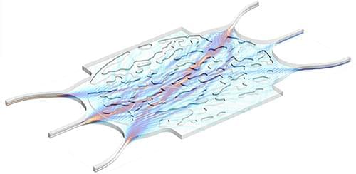
In a new study, scientists from Singapore and Spain have presented a new avenue for exploring exotic physics in graphene. They focus on electronic interactions in graphene when it is sandwiched in a three-layer structure which provides a platform to exploit unique electronic band configurations.
Category: materials – Page 139
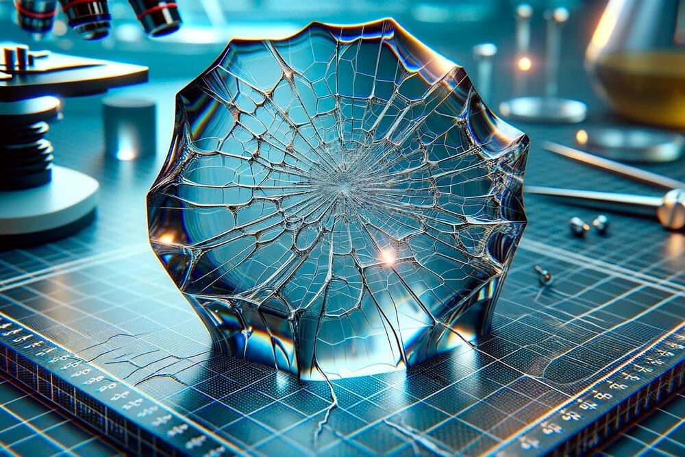
Unlocking the Secrets of Strength Through 3D Crack Analysis
The last time you dropped a favorite mug or sat on your glasses, you may have been too preoccupied to take much notice of the intricate pattern of cracks that appeared in the broken object. But capturing the formation of such patterns is the specialty of John Kolinski and his team at the Laboratory of Engineering Mechanics of Soft Interfaces (EMSI) in EPFL’s School of Engineering. They aim to understand how cracks propagate in brittle solids, which is essential for developing and testing safe and cost-effective composite materials for use in construction, sports, and aerospace engineering.

Electrically Tunable Metasurfaces: Liquid Crystal Alignment by Dielectric Meta-Atoms
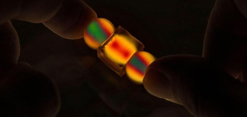
Dielectric metasurfaces, known for their low loss and subwavelength scale, are revolutionizing optical systems by allowing multidimensional light modulation. Researchers have now innovated in this field by developing a liquid crystal-based dielectric metasurface that streamlines manufacturing and enhances device performance.
Dielectric metasurfaces represent one of the cutting-edge research and application directions in the current optical field. They not only possess the advantage of low loss but also enable the realization of device thicknesses at subwavelength scales. Moreover, they can freely modulate light in multiple dimensions such as amplitude, phase, and polarization. This capability, which traditional optics lacks, holds significant importance for the integration, miniaturization, and scaling of future optical systems. Consequently, dielectric metasurfaces have attracted increasing industrial attention.
In this study, Professor Daping Chu’s team at the University of Cambridge developed a novel liquid crystal-based tunable dielectric metasurface. By leveraging the dielectric metasurface’s inherent alignment effect on liquid crystals on top of its electrically controllable properties, the need for liquid crystal alignment layer materials and related processes is eliminated, thus saving device manufacturing time and costs. This has practical implications for devices such as liquid crystal on silicon (LCoS).

Ways Automation Can (And Will) Impact The Manufacturing Industry
Many of us have seen photos of and read stories about robots working on the production floor in factories, speeding up old-school assembly lines to build products more quickly. And while the robotics trend in manufacturing is continuing to grow, that’s not the only way technology (including artificial intelligence) and automation are impacting the industry.
From enhancing worker safety to more efficiently moving goods and materials from point A to point B, automation is making its mark on the manufacturing industry, and tech experts expect even more changes and improvements in the near future. Below, 17 members of Forbes Technology Council discuss specific manufacturing tasks that are (or soon will be) handled more efficiently, safely and productively by technology and automation.
Intel to Build Next-Generation Chips Using ‘Glass Substrate’
Year 2023 face_with_colon_three
The new manufacturing method deals with the packaging substrate, the material to which chip dies are bonded. Intel and others have long used plastic (also known as organic) substrates, but the material can shrink or warp during the chip-making process, leading to defects.
Intel notes the warping risk grows as more silicon is placed on the substrate. “As the demand for data-centric, AI-centric compute increases, we are seeing an increasing amount of silicon being packed onto the package substrate, which organic packages have come to some kind of limitation in terms of handling it,” Manepalli added.
The company found a solution in glass, a homogenous substance that can remain rigid under a higher chip load. “Compared to today’s organic substrates, glass offers distinctive properties such as ultra-low flatness and better thermal and mechanical stability, resulting in much higher interconnect density in a substrate,” Intel said in its announcement.

Strong AI Is A Theoretical Impossibility
Thesis:
Part I: It has been proven that the human mind cannot be analogous to an electronic (or any other type of) computer, and the functioning of an intellective mind cannot be reproduced (though it can certainly be simulated) by any type of mechanical device, including modern artificial intelligence systems.
Part II: It is further impossible that the human mind is a purely material thing (including some “emergent property” of matter).
