These pollutants can originate from many common household products – including vinyl flooring, plastic toys, cleaning products and furniture.
In a significant leap forward for quantum nanophotonics, a team of European and Israeli physicists has introduced a new type of polaritonic cavities and redefined the limits of light confinement. This pioneering work, detailed in a study published in Nature Materials, demonstrates an unconventional method to confine photons, overcoming the traditional limitations in nanophotonics.
Physicists have long been seeking ways to force photons into increasingly small volumes. The natural length scale of the photon is the wavelength and when a photon is forced into a cavity much smaller than the wavelength, it effectively becomes more “concentrated.” This concentration enhances interactions with electrons, amplifying quantum processes within the cavity.
However, despite significant success in confining light into deep subwavelength volumes, the effect of dissipation (optical absorption) remains a major obstacle. Photons in nanocavities are absorbed very quickly, much faster than the wavelength, and this dissipation limits the applicability of nanocavities to some of the most exciting quantum applications.
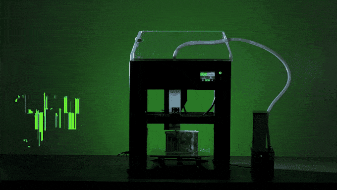
Kickstarter has been the graveyard for several high-profile 3D printers. The crowdfunding platform has also introduced numerous subpar 3D printers, alongside some truly outstanding ones. It was on Kickstarter that Formlabs soared to remarkable heights. The platform also brought us the 3D printing pen. There was a period when a new 3D printing project on Kickstarter emerged every week, but both Kickstarter and additive manufacturing (AM) have become considerably less bustling recently. In 2014, things were simpler, as there were far fewer 3D printers available. Now, with the advent of Bambu Labs and sophisticated open-source 3D printers like Prusas, making a significant impact has become much more challenging. NAW 3D is currently attempting to enter the market with a pellet 3D printer on Kickstarter.
The N300 Pellet 3D Printer
NAW3D’s N300 Desktop Pellet 3D Printer boasts an automatic pellet feeding system, with a 100g capacity consumables box and a 2000cm³ material storage space for continuous printing. Additionally, all axes are equipped with linear guides. What’s more, each stage of the printer incorporates double guides. The printer’s nozzles are capable of reaching temperatures up to 300°C. The print head is designed to deposit substantial amounts of material, with printing tracks ranging from 0.2 to 2mm. This capability suggests that the printer can handle both fine details and rapid, large-scale printing tasks.
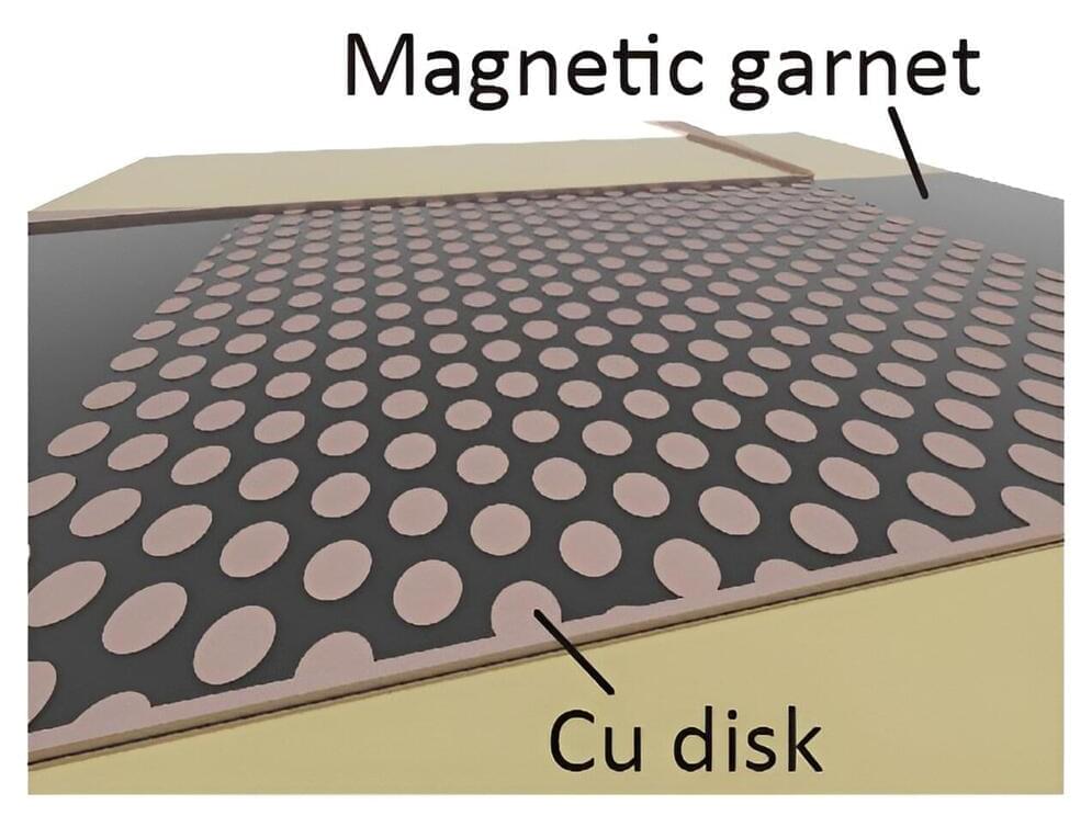
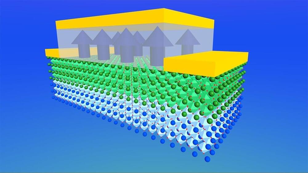
A collaborative group of researchers has potentially developed a means of controlling spin waves by creating a hexagonal pattern of copper disks on a magnetic insulator. The breakthrough is expected to lead to greater efficiency and miniaturization of communication devices in fields such as artificial intelligence and automation technology.
Details of the study were published in the journal Physical Review Applied on January 30, 2024.
In a magnetic material, the spins of electrons are aligned. When these spins undergo coordinated movement, they generate a kind of ripple in the magnetic order, dubbed spin waves. Spin waves generate little heat and offer an abundance of advantages for next-generation devices.
Scientists outline new processes for leveraging hafnia’s ferroelectric features with the aim of enhancing high-performance computing.
Scientists and engineers have been pushing for the past decade to leverage an elusive ferroelectric material called hafnium oxide, or hafnia, to usher in the next generation of computing memory. A team of researchers including the University of Rochester’s Sobhit Singh published a Proceedings of the National Academy of Sciences study outlining progress toward making bulk ferroelectric and antiferroelectric hafnia available for use in a variety of applications.
In a specific crystal phase, hafnia exhibits ferroelectric properties—that is, electric polarization that can be changed in one direction or another by applying an external electric field. This feature can be harnessed in data storage technology. When used in computing, ferroelectric memory has the benefit of non-volatility, meaning it retains its values even when powered off, one of several advantages over most types of memory used today.
New ultrafast method for controlling magnetic materials might enable next-generation information processing technologies.
As demands for computing resources continue to increase rapidly, scientists and engineers are looking for ways to build faster systems for processing information. One possible solution is to use patterns of electron spins, called spin waves, to transfer and process information much more rapidly than in conventional computers. So far, a major challenge has been in manipulating these ultrafast spin waves to do useful work.
Breakthrough in Spin Wave Manipulation.
By better taming the Jekyll-and-Hyde nature of an alternative to the semiconductor—one that transitions from electricity-resisting insulator to current-conducting metal—Nebraska’s Xia Hong and colleagues may have unlocked a new path to smaller, more efficient digital devices. The team reports its findings in the journal Nature Communications.
The semiconductor’s ability to conduct electricity in the Goldilocks zone—poorer than a metal, better than an insulator—positioned it as the just-right choice for engineers looking to build transistors, the tiny on-off switches that encode the 1s and 0s of binary. Apply some voltage to the control knob known as a gate insulator, and the semiconductor channel allows electric current to flow ; remove it, and that flow ceases.
Millions of those nanoscopic, semiconductor-based transistors now coat modern microchips, switching on and off to collectively process or store data. But as minuscule as the transistors already are, the demands of consumers and competition continue pushing electrical engineers to shrink them even further, either for the sake of squeezing in more functionality or downsizing the devices that house them.
The EPFL team, using tellurite glass produced by their Tokyo Tech colleagues, applied their expertise in femtosecond laser technology to alter the glass and study the laser’s effect. After etching a simple line pattern onto a 1 cm diameter tellurite glass and exposing it to UV light and the visible spectrum, Torun found it could generate a current consistently for months.
Bellouard expressed his excitement at the breakthrough, saying, “We’re locally turning glass into a semiconductor using light. We’re essentially transforming materials into something else, perhaps approaching the dream of the alchemist!”
This development may pave the way for windows to function as single-material light-harvesting and sensing devices in the future.

MIT physicists have metaphorically turned graphite, or pencil lead, into gold by isolating five ultrathin flakes stacked in a specific order. The resulting material can then be tuned to exhibit three important properties never before seen in natural graphite.
“It is kind of like one-stop shopping,” says Long Ju, an assistant professor in the Department of Physics and leader of the work, which is reported in the Oct. 5 issue of Nature Nanotechnology. “Nature has plenty of surprises. In this case, we never realized that all of these interesting things are embedded in graphite.”
Further, he says, “It is very rare material to find materials that can host this many properties.”