БЛОГ

Archive for the ‘materials’ category: Page 16

Oct 4, 2024

A Janus Adhesive Hydrogel with Integrated Attack and Defense for Bacteria Killing and Antifouling

Posted by in category: materials

JUST PUBLISHED: A Janus Adhesive Hydrogel with Integrated Attack and Defense for Bacteria Killing and Antifouling.

Oct 2, 2024

Glow in the dark gemstones show the jewellery industry that laboratory-grown crystals can shine bright

Posted by in categories: innovation, materials

For the last three years,…


A UWE Bristol researcher hopes to revolutionise the jewellery industry and its supply chains with the creation of unique gemstone and jewellery designs with ground-breaking properties — including the world’s first single stone glow-in-the-dark manmade crystal.

For the last three years, award-winning jewellery designer Sofie Boons, who’s a Crafts Council Research Fellow at the university’s Centre for Print Research (CFPR), has been undertaking tests on the viability, limitations and use of innovative and experimentally grown crystals in the production of contemporary jewellery.

Continue reading “Glow in the dark gemstones show the jewellery industry that laboratory-grown crystals can shine bright” »

Oct 1, 2024

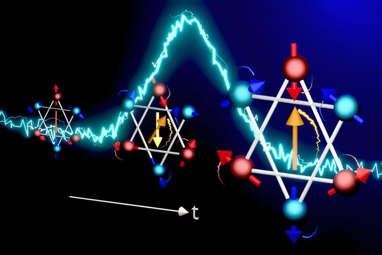
Orbitronics: New Material Property Could Advance Energy-Efficient Tech

Posted by in categories: energy, materials

Yet despite the attraction of OAM monopoles for orbitronics, until this latest study, they have remained a theoretical dream.

Hedgehogs hide between theory and experiment.

To observe them experimentally, hope has lain with a technique known as Circular Dichroism in Angle-Resolved Photoemission Spectroscopy, or CD-ARPES, using circularly polarised X-rays from a synchrotron light source. Yet a gap between theory and experiment has in the past hindered researchers from interpreting the data. “Researchers may have had the data, but the evidence for OAM monopoles was buried in it,” says Schüler.

Sep 29, 2024

Why we are finally within reach of a room-temperature superconductor

Posted by in categories: innovation, materials

A practical superconductor would transform the efficiency of electronics. After decades of hunting, several key breakthroughs are inching us very close to this coveted prize.

By Jon Cartwright

Sep 27, 2024

Simultaneous detection of uranium isotopes and fluorine advances nuclear nonproliferation monitoring

Posted by in categories: materials, particle physics

Combining two techniques, analytical chemists at the Department of Energy’s Oak Ridge National Laboratory have become the first to detect fluorine and different isotopes of uranium in a single particle at the same time. Because fluorine is essential for converting uranium into a form suitable for enrichment, spotting both elements together may help inspectors of the International Atomic Energy Agency, or IAEA, determine the intended use of a nuclear material.

Sep 26, 2024

Researchers develop new p-type semiconductor materials for next-gen displays

Posted by in categories: computing, materials

A group of Korean researchers have recently succeeded in developing new p-type semiconductor materials and thin-film transistors that will lead the innovation of the semiconductor industry. These new discoveries are expected to be widely utilized to improve the overall performance of next-gen displays and ultra-low power semiconductor devices.

Sep 25, 2024

Microchip Breakthrough: This New Material Will Change Everything

Posted by in categories: computing, materials

The first 200 of you will receive the first month of a Planet Wild membership from me for free. Click on this link https://planetwild.com/r/anastasiinte… use the code ANASTASI29 later. You can cancel at any time. If you want to see how Planet Wild works first, check out their latest YouTube video link https://planetwild.com/r/anastasiinte

The video I mentioned about NVIDIA:
➜ • New Nvidia Chip Has a HUGE Problem.

Continue reading “Microchip Breakthrough: This New Material Will Change Everything” »

Sep 25, 2024

Danish physicists make monumental quantum mechanics discovery

Posted by in categories: materials, quantum physics

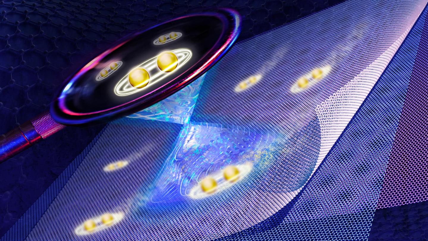
The research was conducted at the Danish National Research Foundation’s “Center of Excellence for Hybrid Quantum Networks (Hy-Q)” and is a collaboration between Ruhr University Bochum in Germany and the University of Copenhagen’s Niels Bohr Institute.

Note: Materials provided above by the The Brighter Side of News. Content may be edited for style and length.

Sep 23, 2024

Water-free manufacturing approach could help advance 2D electronics integration

Posted by in categories: life extension, materials

The future of technology has an age-old problem: rust. When iron-containing metal reacts with oxygen and moisture, the resulting corrosion greatly impedes the longevity and use of parts in the automotive industry. While it’s not called “rust” in the semiconductor industry, oxidation is especially problematic in two-dimensional (2D) semiconductor materials, which control the flow of electricity in electronic devices, because any corrosion can render the atomic-thin material useless. Now, a team of academic and enterprise researchers has developed a synthesis process to produce a “rust-resistant” coating with additional properties ideal for creating faster, more durable electronics.

The team, co-led by researchers at Penn State, published their work in Nature Communications (“Tailoring amorphous boron nitride for high-performance two-dimensional electronics”).

These materials are made from molybdenum disulfide, a two-dimensional semiconductor, grown on a sapphire surface. The triangular shapes seen are aligned because of a special process called epitaxy, where the material follows the pattern of the surface it’s grown on. Insulating layers, like amorphous boron nitride, are added during the process of making these ultra-thin materials, which are used to build next-generation electronic devices. (Image: J.A. Robinson Research Group/Penn State)

Sep 23, 2024

Analyzing Friction in Layered Materials

Posted by in categories: materials, particle physics

Experiments reveal the factors that determine the friction between the single-atom-thick layers in van der Waals materials, which may have uses in lubrication technology.

Van der Waals (vdW) materials consist of stacked, single-atom-thick layers, and these layers can experience very low friction as they slide over one another, a property that might be exploited for lubrication. A research team has now distinguished several contributions to this low friction and has shown that effects at the edges of the sliding regions dominate [1]. Some of their experiments involved sliding a several-layer-thick flake across a surface made of a similar material containing a crack, which allowed the team to systematically control the edge length. The findings could guide efforts to engineer controllable frictional forces into such materials in micromechanical devices.

The very low friction, called superlubricity, exhibited by vdW materials has been previously shown to depend on the relative orientations of the layers. If one layer is rotated by some angle, called the twist angle, with respect to the layer below, the two layers form a “superlattice” in which the two atomic lattices fall periodically in and out of registry, like a pair of overlaid combs with slightly different spacings. This arrangement is called a Moiré pattern, and the repeating elements, or unit cells, of the superlattice are called Moiré tiles. Superlubricity arises because, in general, the contributions to the frictional force from the atoms within one Moiré tile cancel each other out: Some exert a push, while others exert a pull.

Page 16 of 308First1314151617181920Last