Provided manufacturers can find enough raw materials to make them | Science & technology.


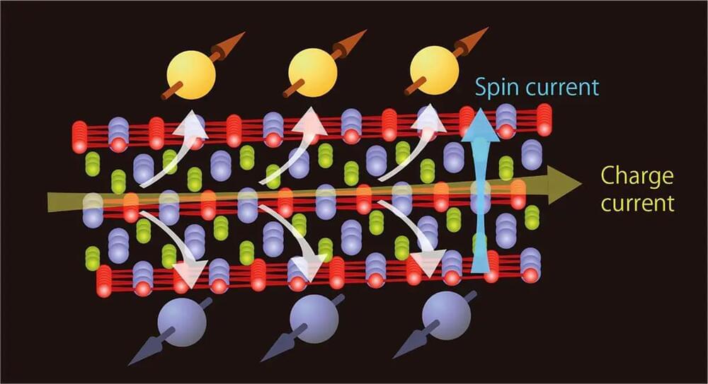
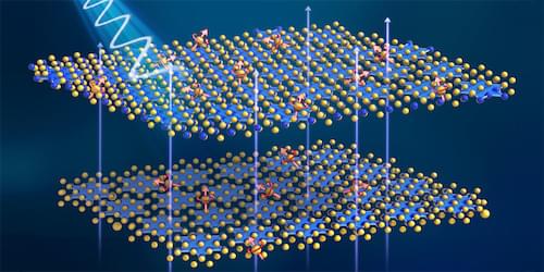
Researchers highlight the potential of cobalt-tin-sulfur in spintronic devices, revealing its capability to reduce energy consumption and heralding a new era in electronics.
A team of researchers has made a significant breakthrough that could revolutionize next-generation electronics by enabling non-volatility, large-scale integration, low power consumption, high speed, and high reliability in spintronic devices.
Details of their findings were published recently in the journal Physical Review B.
X-ray technology plays a vital role in medicine and scientific research, providing non-invasive medical imaging and insight into materials. Recent advancements in X-ray technology enable brighter, more intense beams and imaging of increasingly intricate systems in real-world conditions, like the insides of operating batteries.
To support these advancements, scientists are working to develop X-ray detector materials that can withstand bright, high-energy X-rays—especially those from large X-ray synchrotrons—while maintaining sensitivity and cost-effectiveness.
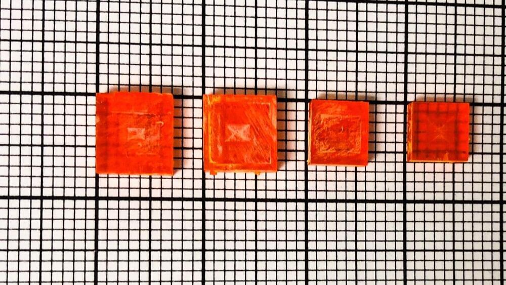
A team of scientists at the U.S. Department of Energy’s (DOE) Argonne National Laboratory and their colleagues have demonstrated exceptional performance of a new material for detecting high energy X-ray scattering patterns. With excellent endurance under ultra-high X-ray flux and relatively low cost, the detector material may find wide application in synchrotron-based X-ray research.
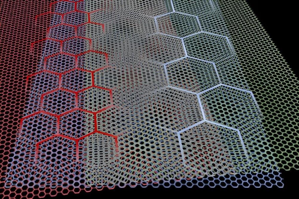
In research that could jumpstart interest into an enigmatic class of materials known as quasicrystals, MIT scientists and colleagues have discovered a relatively simple, flexible way to create new atomically thin versions that can be tuned for important phenomena. In work reported in Nature they describe doing just that to make the materials exhibit superconductivity and more.
The research introduces a new platform for not only learning more about quasicrystals, but also exploring exotic phenomena that can be hard to study but could lead to important applications and new physics. For example, a better understanding of superconductivity, in which electrons pass through a material with no resistance, could allow much more efficient electronic devices.
The work brings together two previously unconnected fields: quasicrystals and twistronics. The latter was pioneered at MIT only about five years ago by Pablo Jarillo-Herrero, the Cecil and Ida Green Professor of Physics at MIT and corresponding author of the paper.

This lightweight material surpasses the strength of steel.
There is a high demand for strong yet lightweight materials across diverse industries, including defense, medical devices, and automotive sectors, among others.
Material scientists have been investigating the possibilities of unconventional components in order to meet this growing demand and enhance technological advancements.
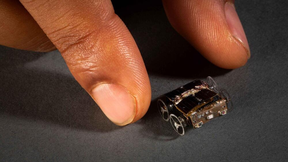
The robot can drive on various surfaces such as concrete or packed soil and carry up to three times its own weight in equipment such as a camera or sensors.
Imagine a tiny robot that can move on its own, powered by light and radio waves. It can carry a camera, a sensor, or a Bluetooth device and transmit data over long distances. It can navigate through different terrains and environments and follow light sources to keep going. It sounds like science fiction, right?
Source: Mark Stone/University of Washington.
Meet MilliMobile

Though a doomed star exploded some 20,000 years ago, its tattered remnants continue racing into space at breakneck speeds—and NASA’s Hubble Space Telescope has caught the action.
The nebula, called the Cygnus Loop, forms a bubble-like shape that is about 120 light-years in diameter. The distance to its center is approximately 2,600 light-years. The entire nebula has a width of six full moons as seen on the sky.
Astronomers used Hubble to zoom into a very small slice of the leading edge of this expanding supernova bubble, where the supernova blast wave plows into surrounding material in space. Hubble images taken from 2001 to 2020 clearly demonstrate how the remnant’s shock front has expanded over time, and they used the crisp images to clock its speed.

A group of researchers from Tohoku University, Massachusetts Institute of Technology (MIT), Rice University, Hanoi University of Science and Technology, Zhejiang University, and Oak Ridge National Laboratory have proposed a new mechanism to enhance short-wavelength light (100–300 nm) by second harmonic generation (SHG) in a two-dimensional (2D), thin material composed entirely of commonplace elements.
Since UV light with SHG plays an important role in semiconductor lithography equipment and medical applications that do not use fluorescent materials, this discovery has important implications for existing industries and all optical applications.
Details of the research were published in the journal ACS Nano on August 29, 2023. The study was selected to be featured on the cover.
A color-changing system inspired by the wings of butterflies can also help scientists provide compound eye vision to robots, but why do scientists want robots to see like insects?
Would you like to try a T-shirt whose color changes with the weather? How about a bandage that alerts you by changing its color when an infection occurs at the site of an injury?
Researchers at the University of Hong Kong have developed a material to turn such ideas into a reality. They have created a rubber-like color-changing system called Morphable Concavity Array (MoCA).