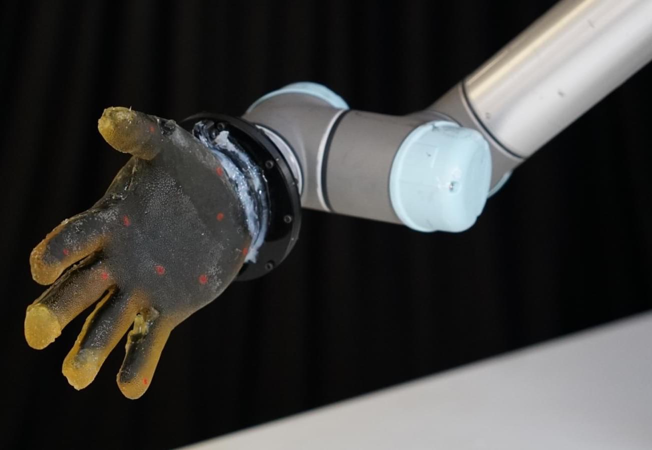
New, gelatin-based material could let robots feel everything from a light poke to a deep cut.

Identifying the formation period of planetary systems, such as our solar system, could be the beginning of the journey to discover the origin of life. The key to this is the unique substructures found in protoplanetary disks—the sites of planet formation.
A protoplanetary disk is composed of low-temperature molecular gas and dust, surrounding a protostar. If a planet exists in the disk, its gravity will gather or eject materials within the disk, forming characteristic substructures such as rings or spirals. In other words, various disk substructures can be interpreted as “messages” from the forming planets. To study these substructures in detail, high-resolution radio observations with ALMA are required.
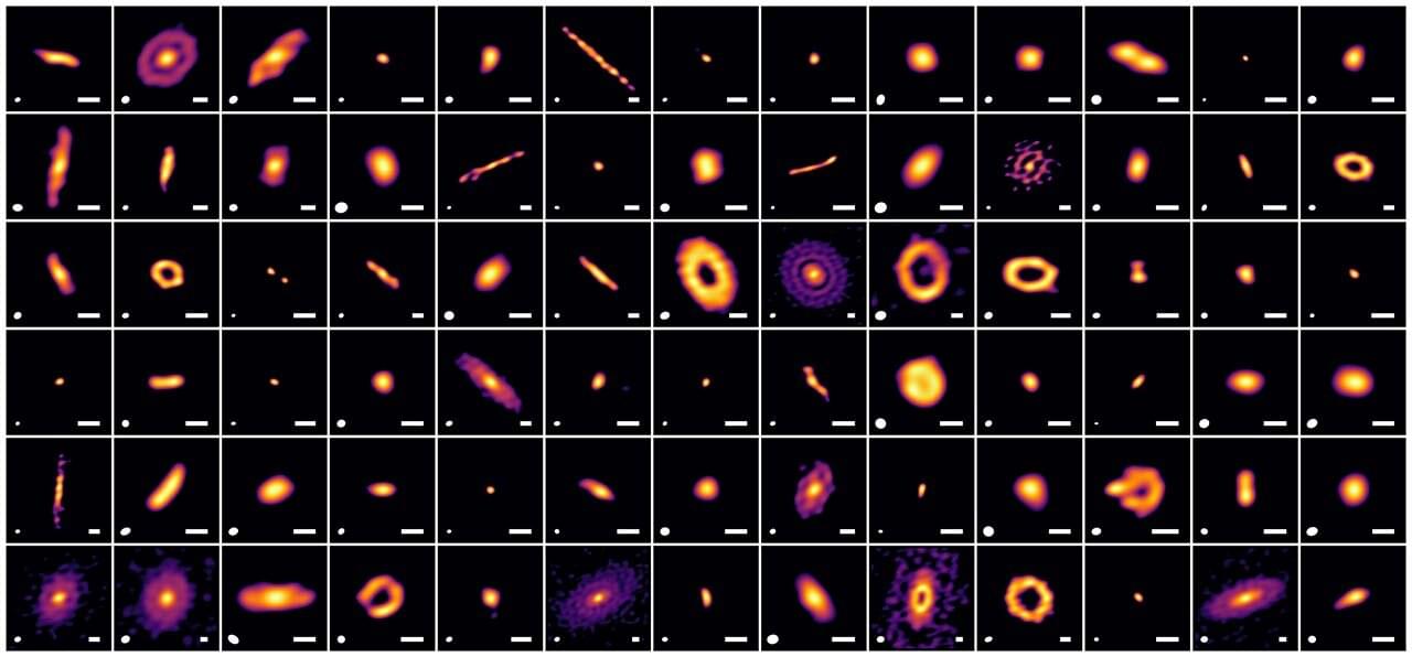
Numerous ALMA observations of protoplanetary disks (or circumstellar disks) have been conducted so far. In particular, two ALMA large programs, DSHARP and eDisk, have revealed the detailed distribution of dust in protoplanetary disks through high-resolution observations.


There are no federal laws regulating A.I. but states have enacted dozens of laws that strengthen consumer privacy, ban A.I.-generated child sexual abuse material and outlaw deepfake videos of political candidates. All but a handful of states have some laws regulating artificial intelligence in place. It is an area of deep interest: All 50 have introduced bills in the past year tied to the issue.
The Senate’s provision, introduced in the Senate by Senator Ted Cruz, Republican of Texas, sparked intense criticism by state attorneys general, child safety groups and consumer advocates who warned the amendment would give A.I. companies a clear runway to develop unproven and potentially dangerous technologies.
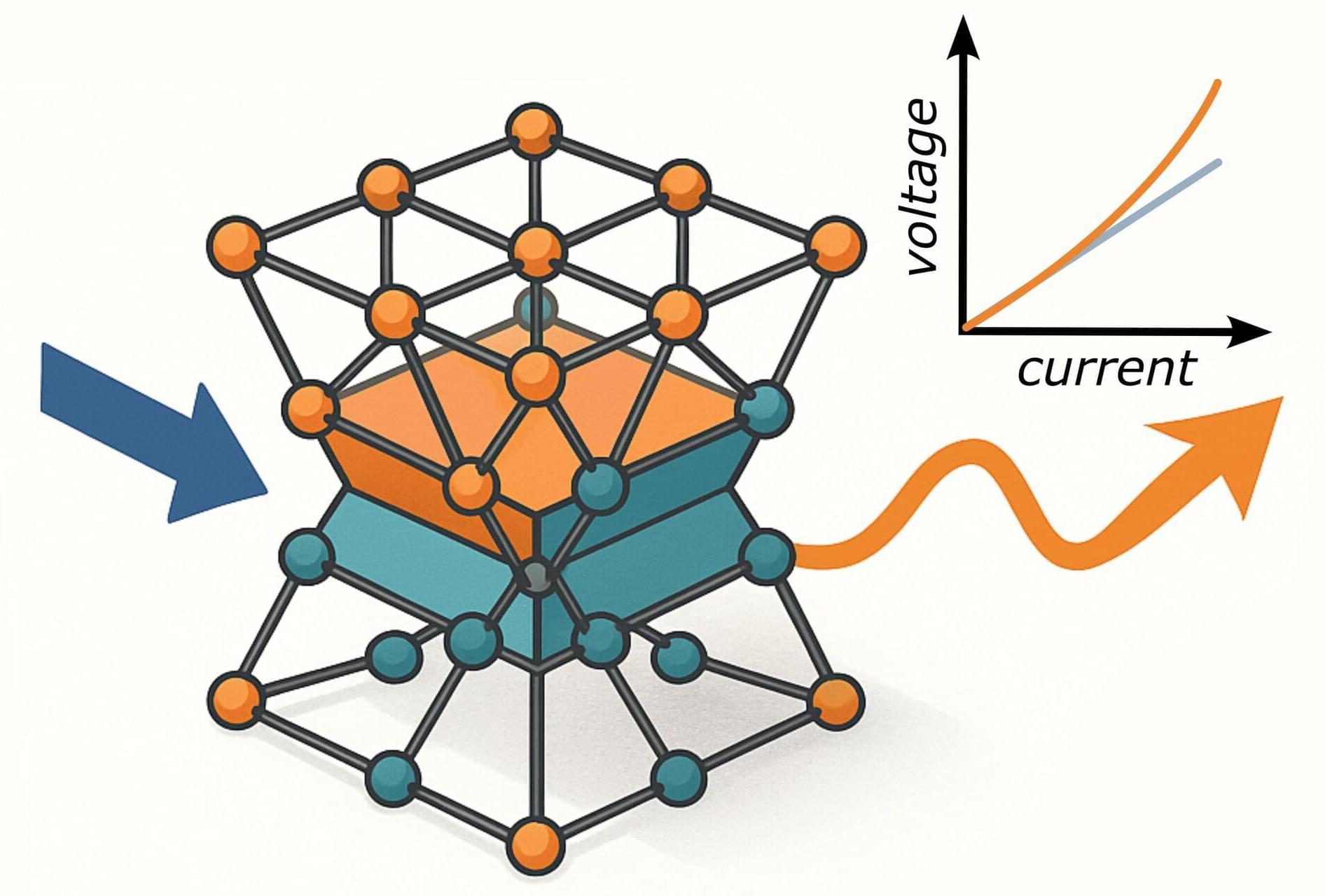
In a review just published in Nature Materials, researchers take aim at the oldest principle in electronics: Ohm’s law.
Their article, “Nonlinear transport in non-centrosymmetric systems,” brings together rapidly growing evidence that, when a material lacks inversion symmetry, the familiar linear relation between current and voltage can break down, giving rise to striking quadratic responses.
The study was led by Manuel Suárez-Rodríguez—working under the guidance of Ikerbasque Professors Fèlix Casanova and Luis E. Hueso at CIC nanoGUNE, together with Prof. Marco Gobbi at the Materials Physics Center (CFM, CSIC-UPV/EHU).

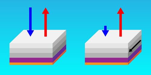
A newly designed structure exhibits the largest-recorded emissivity–absorptivity difference, a property that could prove useful in energy-harvesting and cloaking devices.
Hot objects glow. From the warmth of a stovetop to the invisible heat radiating from a building’s roof, thermal radiation flows outward. But it also flows inward in a reciprocal manner. This means that at thermal equilibrium, an object’s ability to thermally emit light in one direction, described as emissivity, is equal to its ability to absorb the same light coming in from the other direction, known as absorptivity. But what if this rule could be violated?
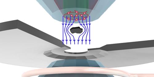
In a new study, Zhenong Zhang and colleagues from Pennsylvania State University demonstrate this exciting possibility [1]. The researchers apply an external magnetic field to a layered material, creating a system that breaks Lorentz reciprocity—a common symmetry that relates electromagnetic inputs and outputs. They then show that this nonreciprocal system exhibits much higher emissivity than absorptivity in the same direction. The observed difference between emissivity and absorptivity is twice that observed in previous experiments, thus setting a new benchmark in the field. These results pave the way for future technologies such as thermal diodes, radiative heat engines, and infrared camouflage.
