Toggle light / dark theme

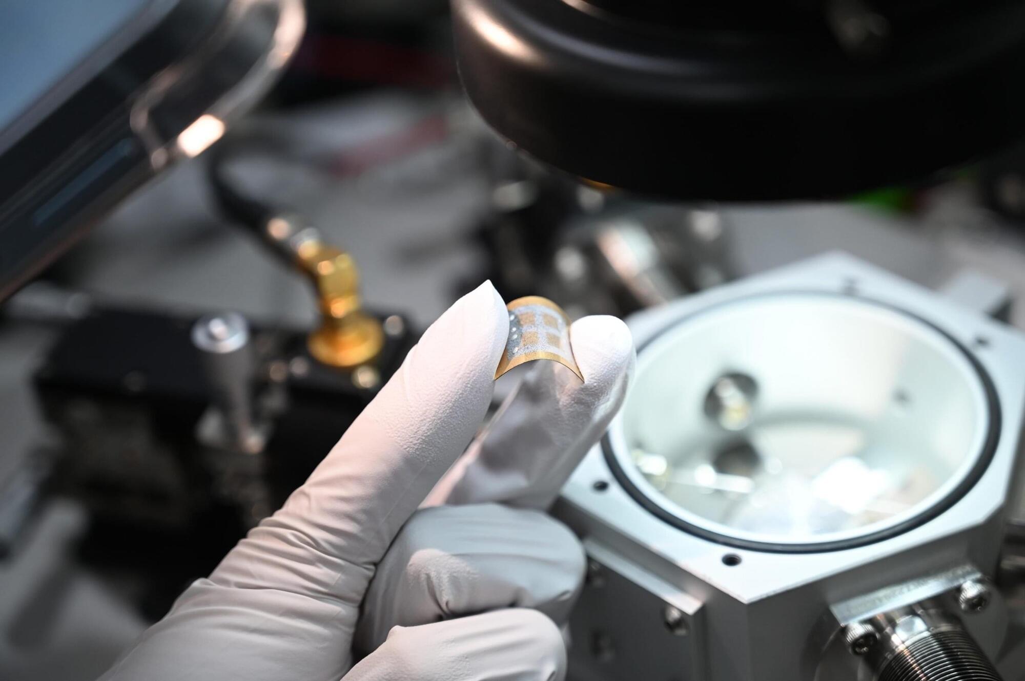
The Sydney team exploited stimulated Brillouin scattering, a technique which involves converting electrical fields into pressure waves in certain insulators, such as optical fibers. In 2011, the researchers reported that Brillouin scattering held potential for high-resolution filtering, and developed new manufacturing techniques to combine a chalcogenide Brillouin waveguide on a silicon chip. In 2023, they managed to combine a photonic filter and modulator on the same type of chip. The combination gives the experimental chip a spectral resolution of 37 megahertz and a wider bandwidth than preceding chips, the team reported in a paper published 20 November in Nature Communications.

“The integration of the modulator with this active waveguide is the key breakthrough here,” says nanophotonics researcher David Marpaung of the University Twente in the Netherlands. Marpaung worked with the Sydney group a decade ago and now leads his own research group that is taking a different approach in the quest to achieve wide-band, high-resolution photonic radio sensitivity in a tiny package. Marpaung says that when someone reaches sub-10-MHz spectral resolution across a 100 gigahertz band, they will be able to replace bulkier electronic RF chips in the marketplace. Another advantage of such chips is that they would convert RF signals to optical signals for direct transmission through fiber optic networks. The winners of that race will be able to reach the huge market of telecoms providers and defense manufacturers who need radio receivers capable of reliably navigating complicated radio-frequency (RF) environments.

“Chalcogenide has a very strong Brillouin effect; it’s very good, but there is still a question of whether this is scalable…it’s still perceived as a lab material,” Marpaung says. The Sydney group had to figure out a new way to fit the chalcogenide waveguides in a 5-millimeter-square package into a standard manufactured silicon chip, which was no easy task. In 2017, the group figured out how to combine chalcogenide onto a silicon input/output ring, but it took until this year for anyone to manage the combination with a standard chip.

Scientists have discovered a new class of materials, carbon nitrides, which could rival diamonds in hardness. This discovery, the result of international collaboration and decades of research, opens up possibilities for various industrial applications due to their durability and other properties like photoluminescence and high energy density. Funded by international grants and published in Advanced Materials, this breakthrough marks a significant advancement in material science.

Scientists have solved a decades-long puzzle and unveiled a near unbreakable substance that could rival diamond, as the hardest material on earth, a study says.

Researchers found that when carbon and nitrogen precursors were subjected to extreme heat and pressure, the resulting materials – known as carbon nitrides – were tougher than cubic boron nitride, the second hardest material after diamond.

The National Institute for Materials Science (NIMS) has succeeded in directly observing the “anisotropic magneto-Thomson effect,” a phenomenon in which the heat absorption/release proportional to an applied temperature difference and charge current (i.e., Thomson effect) changes anisotropically depending on the magnetization direction in magnetic materials.

This research is expected to lead to further development of basic physics and related to the fusion area of thermoelectrics and spintronics, as well as to the development of new functionalities to control with magnetism. The study is published in the journal Physical Review Letters.

The Thomson effect has long been known as one of the fundamental thermoelectric effects in metals and semiconductors, along with the Seebeck and Peltier effects, which are driving principles of thermoelectric conversion technologies.

Over the past few years, engineers have been trying to devise alternative hardware designs that would allow a single device to both perform computations and store data. These emerging electronics, known as computing-in-memory devices, could have numerous advantages, including faster speeds and enhanced data analysis capabilities.

To store data safely and retain a , these devices should be based on with advantageous properties and that can be scaled down in terms of thickness. Two-dimensional (2D) semiconductors that exhibit a property known as sliding ferroelectricity have been found to be promising candidates for realizing computing-in-memory, yet attaining the necessary switchable electric polarization in these materials can prove difficult.

Researchers at National Taiwan Normal University, Taiwan Semiconductor Research Institute, National Yang Ming Chiao Tung University and National Cheng Kung University recently devised an effective strategy to achieve a switchable electric polarization in molybdenum disulfide (MoS2). Using this method, outlined in a Nature Electronics paper, they ultimately developed new promising ferroelectric transistors for computing-in-memory applications.

TL;DR: a warp trip will show up on a gravitational detector because the space ship’s mass instantly disappears and later re-appears somewhere else.

There is some interesting foundational research [ALC] into faster than light [FTL] travel, but by everything these theories tell us, the ingredients for such modes of transportation aren’t available in the universe. FTL should be possible because the universe expands [EXP] at speeds greater than that of light, as [EXP] eloquently states: “galaxies that are farther than the Hubble radius, approximately 4.5 gigaparsecs or 14.7 billion light-years, away from us have a recession speed that is faster than the speed of light”

Since it is unclear whether the material needed for an FTL drive will ever be available, funding research in that direction could be a waste of resources, unless synergies emerge. In the spirit of respecting taxpayer’s money, I think FTL research should try to exploit – and generate – synergies with other fields of research.

McGill University researchers have made a breakthrough in diagnostic technology, inventing a ‘lab on a chip’ that can be 3D-printed in just 30 minutes. The chip has the potential to make on-the-spot testing widely accessible.

As part of a recent study, the results of which were published in the journal Advanced Materials, the McGill team developed capillaric chips that act as miniature laboratories.

Unlike other computer microprocessors, these chips are single-use and require no external power source — a simple paper strip suffices.