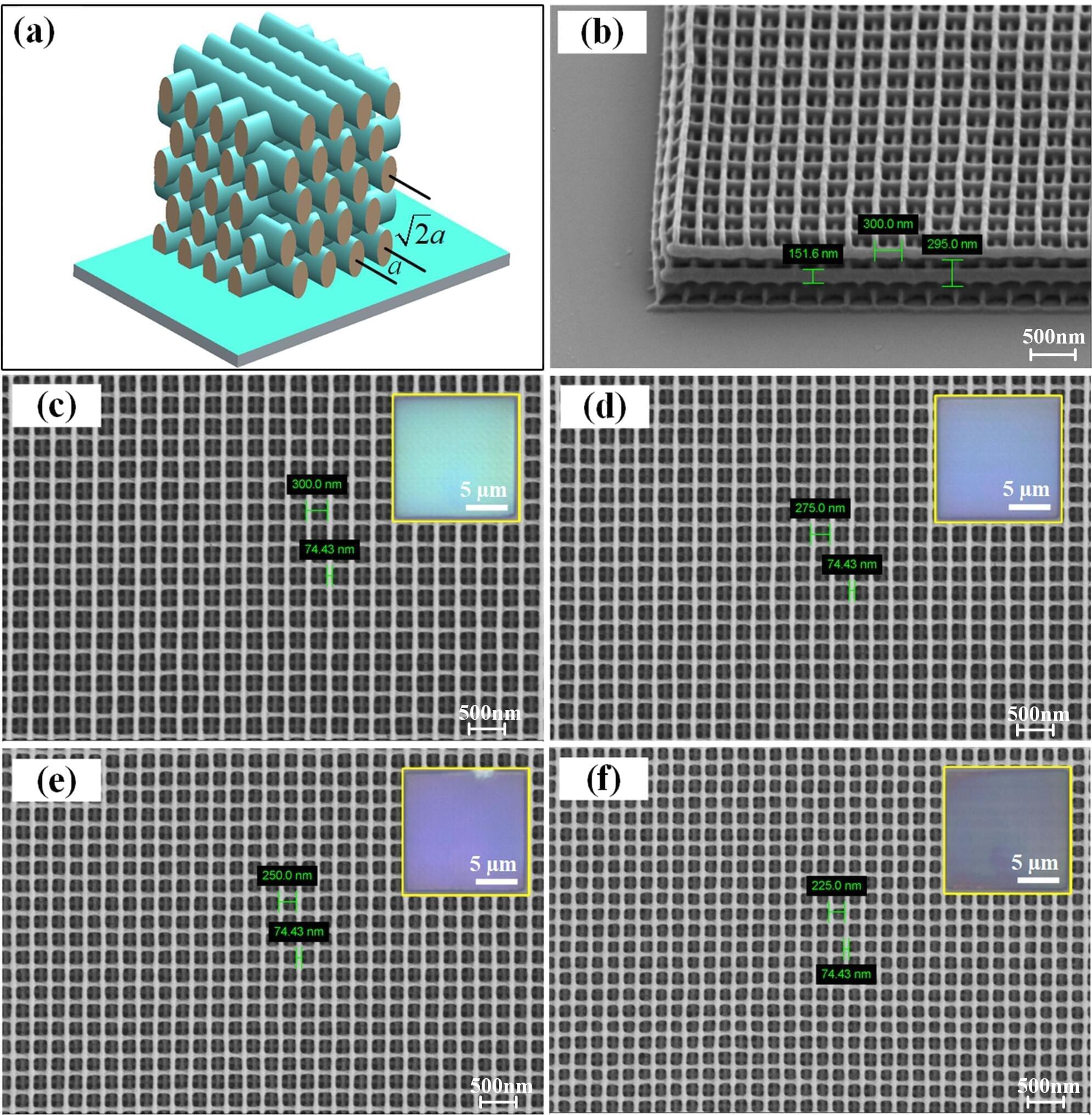
Toggle light / dark theme

The speed of light can be intentionally reduced in various media. Various techniques have been developed over the years to slow down light, including electromagnetically induced transparency (EIT), Bose-Einstein condensate (BEC), photonic crystals, and stimulated Brillouin scattering (SBS).

Notably, researchers from Harvard, led by Lene Vestergaard Hau, reduced light speed to 17 m/s in an ultracold atomic gas using EIT, which sparked the interest in exploring EIT analogs in metasurfaces, a transformative platform in optics and photonics.

Despite the benefits, slow-light structures face a significant challenge: Loss, which limits storage time and interaction length. This issue is particularly severe for analogs of EIT due to scattering loss of nanoparticles and sometimes absorption loss of materials.

Advanced Quantum Technologies is a peer reviewed journal that has published a paper – Global Room-Temperature Superconductivity in Graphite. The researchers are from Brazil, Italy and Switzerland.

They use the scotch-taped cleaved pyrolytic graphite carrying the wrinkles that resulted from this cleaving to which they also refer as to line defects. They detected experimental evidence for the global zero-resistance state. The experimental data clearly demonstrated that the array of nearly parallel linear defects that form due to the cleaving of the highly oriented pyrolytic graphite hosts one-dimensional superconductivity.

One-Dimensional room temperture and room pressure superconductivity is what part of the theory and claims proposed for LK99 and sulfurized LK99 and PCPOSOS.

The team was thrilled with this discovery and saw the potential for creating durable patterns on the glass surface that could produce electricity when illuminated. This is a significant breakthrough because the technique does not require any additional materials, and all that is needed is tellurite glass and a femtosecond laser to create an active photoconductive material.

“Tellurium being semiconducting, based on this finding we wondered if it would be possible to write durable patterns on the tellurite glass surface that could reliably induce electricity when exposed to light, and the answer is yes,” explains Yves Bellouard who runs EPFL’s Galatea Laboratory.

Scientists used a laser-based technique to reveal hidden quantum properties of the material Ta2NiSe5, potentially advancing the development of quantum light sources.

Certain materials have desirable properties that are hidden, and just as you would use a flashlight to see in the dark, scientists can use light to uncover these properties.

Researchers at the University of California San Diego have used an advanced optical technique to learn more about a quantum material called Ta2NiSe5 (TNS). Their work was published in the journal Nature Materials.

A team of researchers from the Institute for Optoelectronic Systems and Microtechnology at Universidad Politécnica de Madrid (UPM) has designed a biosensor capable of identifying proteins and peptides in quantities as low as a single monolayer. For that, a surface acoustic wave (SAW), a kind of electrically controlled nano earthquake on a chip, is generated with an integrated transducer to act on a stack of 2D materials coated with the biomolecules to be detected.

As they report in the journal Biosensors and Bioelectronics in an article titled “Surface–-driven graphene plasmonic sensor for fingerprinting ultrathin biolayers down to the monolayer limit,” the SAW would ripple the surface of a graphene-based stack in such a way that it confines mid– to very small volumes, enhancing at the nanoscale.

In particular, quasiparticles that are part light (photons) and part matter (electrons and lattice vibrations), called surface plasmon-phonon polaritons, are formed at the rippled stack interplaying strongly with the molecules atop.

Researchers have developed a new spectroscopy method to study ultrafast processes in strongly correlated materials, achieving sub-femtosecond resolution.

An international team of researchers from the European XFEL together with colleagues from the Max Born Institute in Berlin, the Universities of Berlin and Hamburg, The University of Tokyo, the Japanese National Institute of Advanced Industrial Science and Technology (AIST), the Dutch Radboud University, Imperial College London, and Hamburg Center for Ultrafast Imaging, have presented new ideas for ultrafast multi-dimensional spectroscopy of strongly correlated solids. This work will be published today (January 24) in Nature Photonics.

Exploring Strongly Correlated Solids