Toggle light / dark theme

A greener, cleaner way to extract cobalt from ‘junk’ materials

Siddarth Kara’s bestseller, “Cobalt Red: How the Blood of Congo Powers Our Lives,” focuses on problems surrounding the sourcing of cobalt, a critical component of lithium-ion batteries that power many technologies central to modern life, from mobile phones and pacemakers to electric vehicles.

“Perhaps many of us have read how are vital for energy storage technologies,” says Eric Schelter, the Hirschmann-Makineni Professor of Chemistry at the University of Pennsylvania. “But how materials that make up such batteries are sourced can be concerning and problematic, both ethically and environmentally.”

Schelter says that mining in the Democratic Republic of Congo, which supplies about 70% of the world’s cobalt, raises concerns due to environmental degradation and unsafe working conditions, and that large-scale mining disrupts ecosystems and can contaminate , leaving lasting environmental damage. In addition, he notes that a looming cobalt shortage threatens to strain as demand for battery technologies continues to grow.

LEDs Based on Transition Metal Dichalcogenides Display Reduced Efficiency Losses

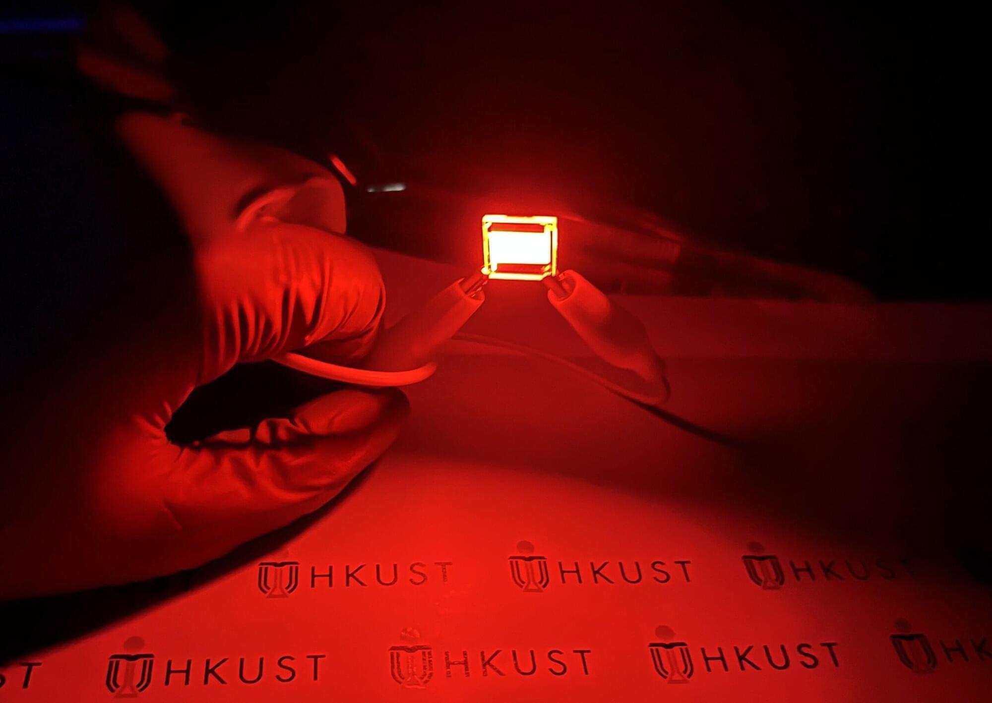
Light-emitting diodes (LEDs), semiconductor-based devices that emit light when an electric current flows through them, are key building blocks of numerous electronic devices. LEDs are used to light up smartphone, computer, and TV displays, as well as light sources for indoor and outdoor environments.

Past studies consistently observed a decline in the performance and efficiency of LED devices based on two-dimensional (2D) materials at high current densities. This loss of efficiency at high current densities has been linked to high levels of interaction between excitons, which cause a process known as exciton-exciton annihilation (EEA).

Essentially, the properties of some 2D materials prompt excitons to strongly interact with each other, causing excitons to “deactivate” one another. This results in a significant waste of energy that could otherwise contribute to the lighting of LEDs.

Millions of smartphones monitor Earth’s ever-changing ionosphere

A plan to use millions of smartphones to map out real-time variations in Earth’s ionosphere has been tested by researchers in the US. Developed by Brian Williams and colleagues at Google Research in California, the system could improve the accuracy of global navigation satellite systems (GNSSs) such as GPS and provide new insights into the ionosphere.

\r \r.

A GNSS uses a network of satellites to broadcast radio signals to ground-based receivers. Each receiver calculates its position based on the arrival times of signals from several satellites. These signals first pass through Earth’s ionosphere, which is a layer of weakly-ionized plasma about 50–1500 km above Earth’s surface. As a GNSS signal travels through the ionosphere, it interacts with free electrons and this slows down the signals slightly – an effect that depends on the frequency of the signal.

Inspired by nature: Leaftronics pave way for biodegradable electronics

A research team headed by Prof. Karl Leo at TUD Dresden University of Technology have developed an innovative, nature-inspired solution that could revolutionize the electronics industry: “Leaftronics.” This innovative approach leverages the natural structure of leaves to create biodegradable electronic substrates with enhanced properties and offers a sustainable, efficient, and scalable solution to the global-waste problem. These findings have now been published in the journal Science Advances.

Electronic devices, from toys to smartphones, consist of circuits. Specific substrates are used to manufacture these circuits. In commercial electronics, these are printed circuit boards (PCBs) made of glass fiber-reinforced epoxy resin.

Most of these materials are not recyclable, let alone biodegradable. Given the sheer volume of electronic waste of more than 60 million tons per year (of which over 75% is not collected worldwide), there is an urgent need for sustainable alternatives.

New Material to make Next Generation of Electronics Faster and More Efficient

With the increase of new technology and artificial intelligence, the demand for efficient and powerful semiconductors continues to grow. Researchers at the University of Minnesota have achieved a new material that will be pivotal in making the next generation of high-power electronics faster, transparent and more efficient. This artificially designed material allows electrons to move faster while remaining transparent to both visible and ultraviolet light, breaking the previous record.

The research, published in Science Advances, a peer-reviewed scientific journal, marks a significant leap forward in semiconductor design, which is crucial to a trillion-dollar global industry expected to continue growing as digital technologies expand.

Semiconductors power nearly all electronics, from smartphones to medical devices. A key to advancing these technologies lies in improving what scientists refer to as “ultra-wide band gap” materials. These materials can conduct electricity efficiently even under extreme conditions. Ultra-wide band gap semiconductors enable high-performance at elevated temperatures, making them essential for more durable and robust electronics.

Wireless ultrasonic knife glides through most things like butter

From a handheld soldering gun to the ‘playbird mansion’ and, of course, the marvel of a smartphone microscope, there are some gadgets that we come across that we instantly want – and this wireless ultrasonic cutter is definitely another.

And much like the soldering gun, this little jigger has such a broad range of applications that, while it’s aimed at the do-it-yourself maker and crafter, its appeal is certainly not limited to this.

The Hanboost C1 wireless ultrasonic cutter can precisely slice through a vast array of materials – wood, plastics, leather, rubber, paper – silently, using 40,000 vibrations per second to make even the most fiddly jobs look easy. No tearing, no scratching or scoring, it just glides through calmly, slowly and with effortless precision.

An efficient small language model that could perform better on smartphones

There are over 30,000 weather stations in the world, measuring temperature, precipitation and other indicators often on a daily basis. That’s a massive amount of data for climate researchers to compile and analyze to produce the monthly and annual global and regional temperatures (especially) that make the news.

Now researchers have unleashed artificial intelligence (AI) on these datasets to analyze in Europe, finding excellent agreement compared to existing results that used traditional methods, and as well have uncovered climate extremes not previously known. Their work has been published in Nature Communications.

With the world’s climate changing rapidly, it is important to know how temperature and precipitation extremes are changing, so planners can adapt to the extremes here now and to what’s coming.

US scientists may have developed the first robot syllabus that allows machines to transfer skills without human intervention

Whether it’s our phones, cars, televisions, medical devices or even washing machines, we now have computers everywhere.

Using bigger computers, we solve bigger problems like managing the operation of a power grid, designing an aircraft, predicting the weather or providing different types of artificial intelligence (AI).

But all these machines work by manipulating data in the form of ones and zeros (bits) using classical techniques that have not changed since the abacus was invented in antiquity.

Breakthrough Material Perfectly Absorbs All Electromagnetic Waves

A new composite material developed by KIMS researchers absorbs over 99% of electromagnetic waves from different frequencies, improving the performance of devices like smartphones and wearables.

A team of scientists from the Korea Institute of Materials Science (KIMS) has developed the world’s first ultra-thin film composite material capable of absorbing over 99% of electromagnetic waves from various frequency bands, including 5G/6G, WiFi, and autonomous driving radar, using a single material.

This novel electromagnetic wave absorption and shielding material is less than 0.5mm thick and is characterized by its low reflectance of less than 1% and high absorbance of over 99% across three different frequency bands.