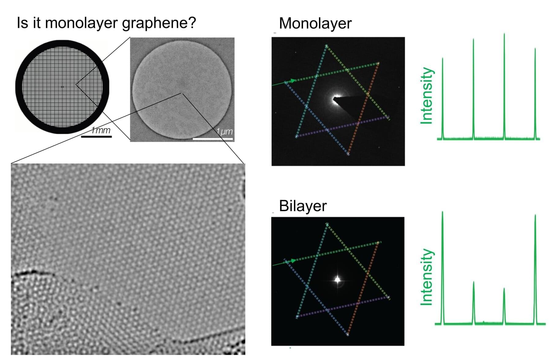
Toggle light / dark theme

A new study published in Frontiers in Computer Science investigated if placing smartphones just out of our reach while we’re at work influenced device use for activities not related to work.

“The study shows that putting the smartphone away may not be sufficient to reduce disruption and procrastination, or increase focus,” said the paper’s author Dr. Maxi Heitmayer, a researcher at the London School of Economics. “The problem is not rooted within the device itself, but in the habits and routines that we have developed with our devices.”

Researchers from the National University of Singapore (NUS) have demonstrated that a single, standard silicon transistor, the fundamental building block of microchips used in computers, smartphones and almost every electronic system, can function like a biological neuron and synapse when operated in a specific, unconventional way.

Led by Associate Professor Mario Lanza from the Department of Materials Science and Engineering at the College of Design and Engineering, NUS, the research team’s work presents a highly scalable and energy-efficient solution for hardware-based (ANNs).

This brings —where chips could process information more efficiently, much like the —closer to reality. Their study was published in the journal Nature.

Imagine navigating a virtual reality with contact lenses or operating your smartphone underwater: This and more could soon be a reality thanks to innovative e-skins.

A research team led by the Helmholtz-Zentrum Dresden-Rossendorf (HZDR) has developed an that detects and precisely tracks magnetic fields with a single global sensor. This artificial skin is not only light, transparent and permeable, but also mimics the interactions of real skin and the brain, as the team reports in the journal Nature Communications.

Originally developed for robotics, e-skins imitate the properties of real skin. They can give robots a or replace lost senses in humans. Some can even detect chemical substances or magnetic fields. But the technology also has its limits. Highly functional e-skins are often impractical because they rely on extensive electronics and large batteries.

Imagine never charging your phone again or having a pacemaker that lasts a lifetime. Scientists are developing tiny nuclear batteries powered by radiocarbon, a safe and abundant by-product of nuclear plants.

Unlike lithium-ion batteries, which degrade over time and harm the environment, these new designs use beta radiation to trigger an electron avalanche and generate electricity. The team’s latest prototype vastly improved efficiency, and though challenges remain, the technology could one day make nuclear power as accessible as your pocket device.

The Problem with Current Batteries.

Sometimes cell phones die sooner than expected or electric vehicles don’t have enough charge to reach their destination. The rechargeable lithium-ion (Li-ion) batteries in these and other devices typically last hours or days between charging. However, with repeated use, batteries degrade and need to be recharged more frequently.

New sapphire nanostructures created at UT Austin repel dust, glare, and fog while staying durable. Inspired by nature, these surfaces could be used in electronics, optics, space, and defense, and are being developed for real-world applications. Imagine a phone screen that stays flawless no matter

A visionary who predicted the internet and smartphones is now making an even bolder claim about the future of humanity. Revolutionary technologies could soon make immortality a reality.

The use of smartphones in Japan is extending to younger and younger children, raising serious concerns about the dangers of social media. An online safety expert provides a snapshot of Japanese teens’ use of current platforms and considers the options for protecting children from cyberbullying, exploitation, and toxic content.

Phase changes are central to the world around us. Probably the most familiar example is when ice melts into water or water boils into steam, but phase changes also underlie heating systems and even digital memory, such as that used in smartphones.

Triggered by or electricity, some materials can switch between two different phases that represent binary code 0s and 1s to store information. Understanding how a material transforms from one state or phase to another is key to tailoring materials with specific properties that could, for instance, increase switching speed or operate at lower energy costs.

Yet researchers have never been able to directly visualize how these transformations unfold in real time. We often assume materials are perfect and look the same everywhere, but “part of the challenge is that these processes are often heterogeneous, where different parts of the material change in different ways, and involve many different length scales and timescales,” said Aaron Lindenberg, co-author and SLAC and Stanford University professor.

A group of Carnegie Mellon University researchers recently devised a method allowing them to create large amounts of a material required to make two-dimensional (2D) semiconductors with record high performance. Their paper, published in ACS Applied Materials & Interfaces in late December 2024, could lead to more efficient and tunable photodetectors, paving the way for the next generation of light-sensing and multifunctional optoelectronic devices.

“Semiconductors are the key enabling technology for today’s electronics, from laptops to smartphones to AI applications,” said Xu Zhang, assistant professor of electrical and computer engineering. “They control the flow of electricity, acting as a bridge between conductors (which allow electricity to flow freely) and insulators (which block it).”

Zhang’s research group wanted to develop a certain kind of photodetector, a device capable of detecting light and which can be used in a variety of applications. To create this photodetector, the group needed to use materials that were an atom’s-width thick, or as close to 2D as is possible.