БЛОГ

Archive for the ‘nanotechnology’ category: Page 11

Jul 30, 2024

New, more sustainable method for manufacturing microchips and other nanoscale devices

Posted by in categories: biological, computing, nanotechnology, sustainability

Putting 50 billion transistors into a microchip the size of a fingernail is a feat that requires manufacturing methods of nanometer level precision—layering of thin films, then etching, depositing, or using photolithography to create the patterns of semiconductor, insulator, metal, and other materials that make up the tiny working devices within the chip.

The process relies heavily on solvents that carry and deposit materials in each layer—solvents that can be difficult to handle and toxic to the environment.

Now researchers led by Fiorenzo Omenetto, Frank C. Doble Professor of Engineering at Tufts, have developed a nanomanufacturing approach that uses water as the primary solvent, making it more environmentally compatible and opening the door to the development of devices that combine inorganic and biological materials.

Jul 30, 2024

Scientists ‘Mind Controlled’ Mice Remotely in Extraordinary World First

Posted by in categories: bioengineering, biotech/medical, genetics, nanotechnology, neuroscience

At the mere flick of a magnetic field, mice engineered with nanoparticle-activated ‘switches’ inside their brains were driven to feed, socialize, and act like clucky new mothers in an experiment designed to test an innovative research tool.

While ’mind control’ animal experiments are far from new, they have generally relied on cumbersome electrodes tethering the subject to an external system, which not only requires invasive surgery but also sets limits on how freely the test subject can move about.

In what is claimed to be a breakthrough in neurology, researchers from the Institute for Basic Science (IBS) in Korea have developed a method for targeting pathways in the brain using a combination of genetics, nanoparticles, and magnetic fields.

Jul 29, 2024

Researchers trap atoms, forcing them to serve as photonic transistors

Posted by in categories: computing, engineering, nanotechnology, particle physics, quantum physics, tractor beam

Researchers at Purdue University have trapped alkali atoms (cesium) on an integrated photonic circuit, which behaves like a transistor for photons (the smallest energy unit of light) similar to electronic transistors. These trapped atoms demonstrate the potential to build a quantum network based on cold-atom integrated nanophotonic circuits. The team, led by Chen-Lung Hung, associate professor of physics and astronomy at the Purdue University College of Science, published their discovery in the American Physical Society’s Physical Review X (“Trapped Atoms and Superradiance on an Integrated Nanophotonic Microring Circuit”).

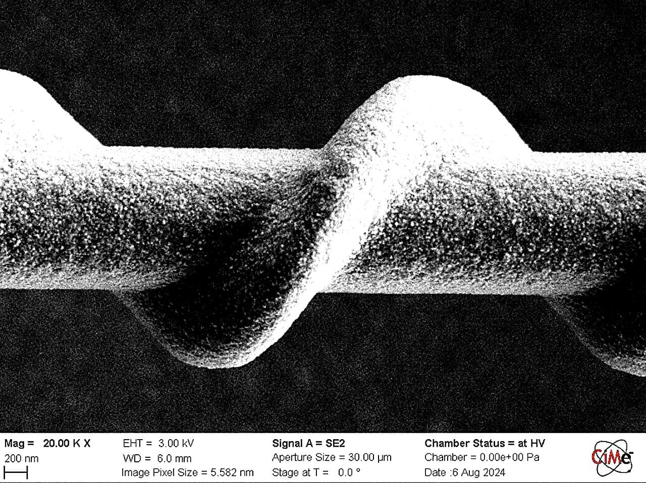
“We developed a technique to use lasers to cool and tightly trap atoms on an integrated nanophotonic circuit, where light propagates in a small photonic ‘wire’ or, more precisely, a waveguide that is more than 200 times thinner than a human hair,” explains Hung, who is also a member of the Purdue Quantum Science and Engineering Institute. “These atoms are ‘frozen’ to negative 459.67 degrees Fahrenheit or merely 0.00002 degrees above the absolute zero temperature and are essentially standing still. At this cold temperature, the atoms can be captured by a ‘tractor beam’ aimed at the photonic waveguide and are placed over it at a distance much shorter than the wavelength of light, around 300 nanometers or roughly the size of a virus. At this distance, the atoms can very efficiently interact with photons confined in the photonic waveguide. Using state-of-the-art nanofabrication instruments in the Birck Nanotechnology Center, we pattern the photonic waveguide in a circular shape at a diameter of around 30 microns (three times smaller than a human hair) to form a so-called microring resonator. Light would circulate within the microring resonator and interact with the trapped atoms.”

A key aspect function the team demonstrates in this research is that this atom-coupled microring resonator serves like a ‘transistor’ for photons. They can use these trapped atoms to gate the flow of light through the circuit. If the atoms are in the correct state, photons can transmit through the circuit. Photons are entirely blocked if the atoms are in another state. The stronger the atoms interact with the photons, the more efficient this gate is.

Jul 27, 2024

Twisted carbon nanotubes could achieve significantly better energy storage than advanced lithium-ion batteries

Posted by in categories: biotech/medical, nanotechnology

An international team of scientists, including two researchers who now work in the Center for Advanced Sensor Technology (CAST) at UMBC, has shown that twisted carbon nanotubes can store three times more energy per unit mass than advanced lithium-ion batteries. The finding may advance carbon nanotubes as a promising solution for storing energy in devices that need to be lightweight, compact, and safe, such as medical implants and sensors. The research was published recently in the journal Nature Nanotechnology.

Jul 26, 2024

Carving Out Nanostructures Beneath the Surface of Silicon

Posted by in categories: computing, nanotechnology, transportation

Modern computer chips can have features built on a nanometer scale. Until now it has been possible to form such small structures only on top of a silicon wafer, but a new technique can now create nanoscale features in a layer below the surface. The approach has promising applications in both photonics and electronics, say its inventors, and could one day enable the fabrication of 3D structures throughout the bulk of the wafer.

The technique relies on the fact that silicon is transparent to certain wavelengths of light. This means the right kind of laser can travel through the surface of the wafer and interact with the silicon below. But designing a laser that can pass through the surface without causing damage and still carry out precise nanoscale fabrication below is not simple.

Researchers from Bilkent University in Ankara, Türkiye, achieved this by using spatial light modulation to create a needlelike laser beam that gave them greater control over where the beam’s energy was deposited. By exploiting physical interactions between the laser light and the silicon, they were able to fabricate lines and planes with different optical properties that could be combined to create nanophotonic elements below the surface.

Jul 26, 2024

Novel optical nanoscopy unveils ultrafast dynamics in nanomaterials

Posted by in categories: materials, nanotechnology

Researchers from the University of California, Berkeley have developed cutting-edge nanoscale optical imaging techniques to provide unprecedented insights into the ultrafast carrier dynamics in advanced materials. Two recent studies, published in Advanced Materials (“Transient Nanoscopy of Exciton Dynamics in 2D Transition Metal Dichalcogenides”) and ACS Photonics (“Near-Field Nanoimaging of Phases and Carrier Dynamics in Vanadium Dioxide Nanobeams”), showcase significant progress in understanding the carrier behaviors in two-dimensional and phase-change materials, with implications for next-generation electronic and optoelectronic devices.

The research team, led by Prof. Costas P. Grigoropoulos, Dr. Jingang Li, and graduate student Rundi Yang, employed a novel near-field transient nanoscopy technique to probe the behavior of materials at the nanoscale with both high spatial and temporal resolution. This approach overcomes the limitations of traditional optical methods, allowing researchers to directly visualize and analyze phenomena that were previously difficult to observe.

Schematic of the near-field transient nanoscopy. (Image: Adapted from DOI:10.1002/adma.202311568, CC BY-NC-ND 4.0)

Jul 26, 2024

Microglia rescue neurons from aggregate-induced neuronal dysfunction and death through tunneling nanotubes

Posted by in categories: biotech/medical, health, nanotechnology, neuroscience

In a recent study published in Neuron, researchers discovered that microglia, the brain’s immune cells, use tunneling nanotubes…


Scheiblich et al. uncover a novel mechanism by which microglia use tunneling nanotubes to connect with α-syn-or tau-burdened neurons, enabling transfer of these proteins to microglia for clearance. Microglia donate mitochondria to restore neuronal health, shedding light on new therapeutic strategies for neurodegenerative diseases.

Jul 26, 2024

New Technology to Control the Brain Using Magnetic Fields Developed

Posted by in categories: biotech/medical, computing, genetics, nanotechnology, neuroscience

Nano-MIND Technology for Wireless Control of Brain Circuits with Potential to Modulate Emotions, Social Behaviors, and Appetite.


Researchers at the Center for Nanomedicine within the Institute for Basic Science (IBS) and Yonsei University in South Korea have unveiled a groundbreaking technology that can manipulate specific regions of the brain using magnetic fields, potentially unlocking the secrets of high-level brain functions such as cognition, emotion, and motivation. The team has developed the world’s first Nano-MIND (Magnetogenetic Interface for NeuroDynamics) technology, which allows for wireless, remote, and precise modulation of specific deep brain neural circuits using magnetism.

The human brain contains over 100 billion neurons interconnected in a complex network. Controlling the neural circuits is crucial for understanding higher brain functions like cognition, emotion, and social behavior, as well as identifying the causes of various brain disorders. Novel technology to control brain functions also has implications for advancing brain-computer interfaces (BCIs), such as those being developed by Neuralink, which aim to enable control of external devices through thought alone.

Continue reading “New Technology to Control the Brain Using Magnetic Fields Developed” »

Jul 26, 2024

Quantum Sensor for the Atomic World Developed through International Scientific Collaboration

Posted by in categories: biotech/medical, nanotechnology, quantum physics

In a scientific breakthrough, an international research team from Korea’s IBS Center for Quantum Nanoscience (QNS) and Germany’s Forschungszentrum Jülich developed a quantum sensor capable of detecting minute magnetic fields at the atomic length scale. This pioneering work realizes a long-held dream of scientists: an MRI-like tool for quantum materials.

The research team utilized the expertise of bottom-up single-molecule fabrication from the Jülich group while conducting experiments at QNS, utilizing the Korean team’s leading-edge instrumentation and methodological know-how to develop the world’s first quantum sensor for the atomic world.

The diameter of an atom is a million times smaller than the thickest human hair. This makes it extremely challenging to visualize and precisely measure physical quantities like electric and magnetic fields emerging from atoms. To sense such weak fields from a single atom, the observing tool must be highly sensitive and as small as the atoms themselves.

Jul 26, 2024

Escaping kinetic traps: How molecular interactions make it possible to overcome the energy barrier

Posted by in categories: energy, nanotechnology, physics

In a paper in Physical Review Letters scientists from the department Living Matter Physics at the Max Planck Institute for Dynamics and Self-Organization (MPI-DS) propose a mechanism on how energy barriers in complex systems can be overcome. These findings can help to engineer molecular machines and to understand the self-organization of active matter.

Page 11 of 303First89101112131415Last